

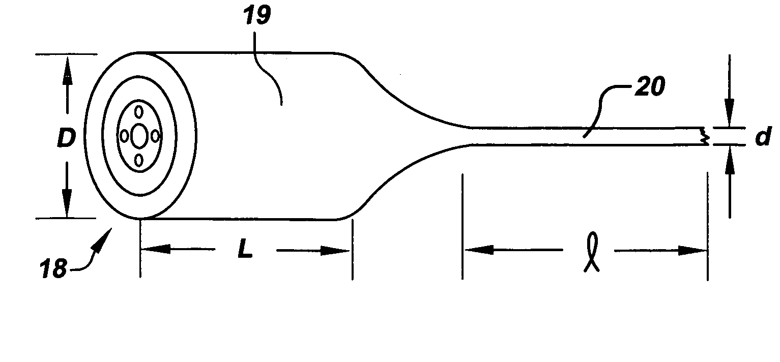
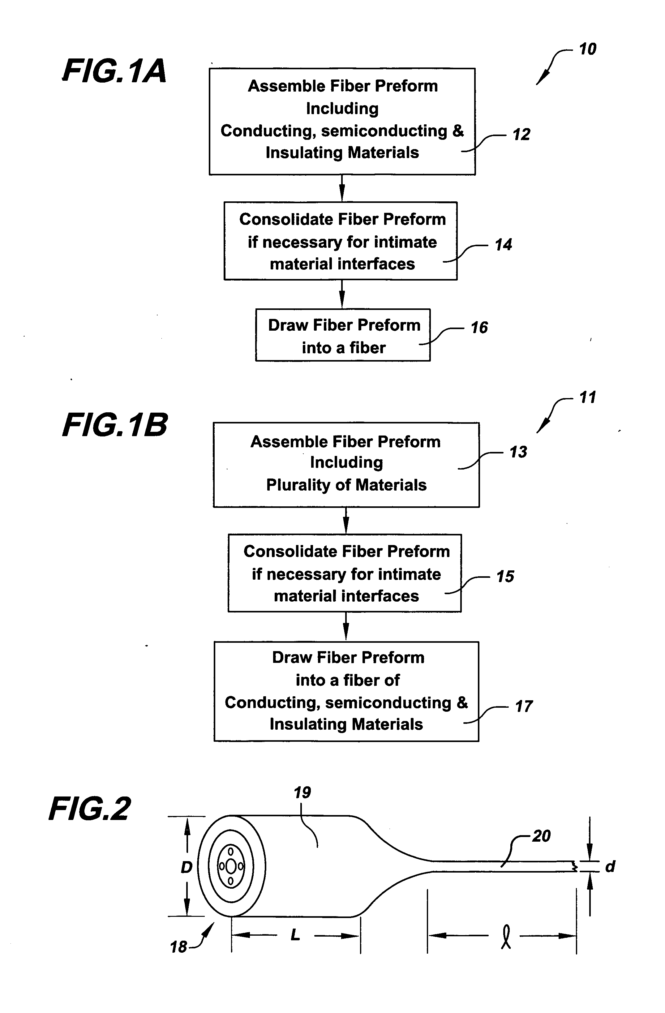
Thermal sensing fiber devices
a technology of thermal sensing fiber and fiber, which is applied in the field of optical fibers, optical devices, electronic devices, optoelectronic devices, etc., can solve the problems of large capital expenditure, limited device extent and/or material coverage area, and restricted microfabrication techniques to planar conformality and planar conformality, etc., to achieve high spatial resolution, facilitate safe and reliable operation, and light weight
- Summary
- Abstract
- Description
- Claims
- Application Information
AI Technical Summary
Benefits of technology
Problems solved by technology
Method used
Image

Examples
example i
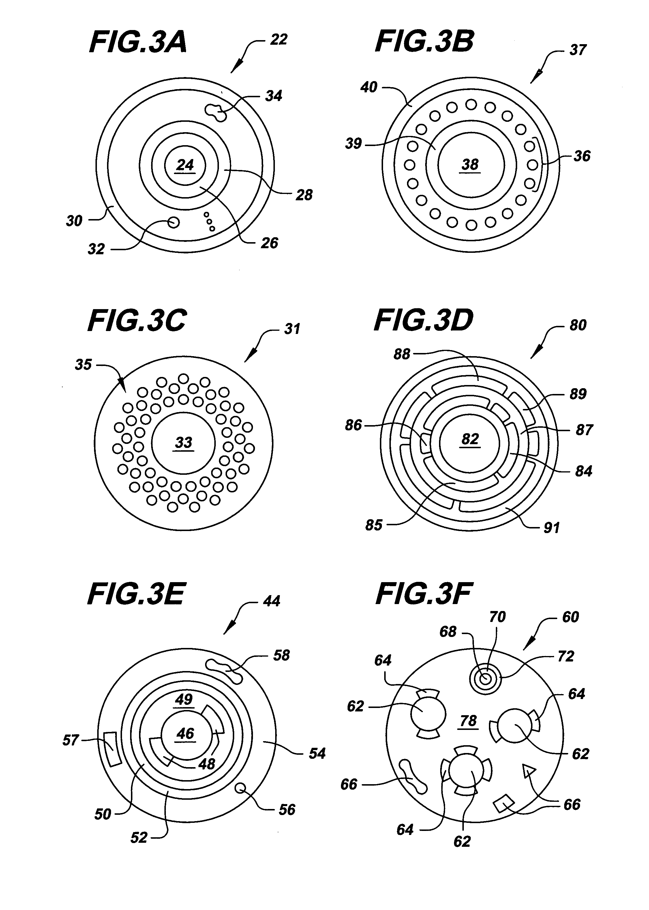
[0136]Referring to FIG. 4, a fiber 90 for conducting both photons and electrons was produced in accordance with the invention. A photon conducting region was provided as a hollow fiber core 92 around which was provided a multilayer photonic bandgap structure 94 of alternating semiconducting and insulating material layers. The bandgap structure exhibited a photonic bandgap at the wavelength corresponding to photon transmission. Sixty cylindrical strands 96 each having an Sn core and polymer cladding were provided around the bandgap structure, and additional polymer reinforcement material 98 was provided around the strands.
[0137]While this example bandgap structure is an omnidirectional reflecting mirror, fibers of the invention are not limited to such; the bandgap structure need not be a multilayer or 1D photonic bandgap structure and instead can exhibit a 2D or 3D photonic bandgap employing structures having periodicities in more than one direction. In the bandgap structure shown, t...
example ii
[0147]Referring now to FIG. 8, a fiber was produced in accordance with the invention configured with a 500 μm diameter semiconducting core region 102 of As2Se3 chalcogenide glass directly contacted by two Sn metal electrodes 104 of 65 μm in radial thickness and 180 μm in circumferential length, along the longitudinal length of the fiber. A layer of PES was provided around the metal electrodes.
[0148]The fiber preform was produced in the manner described previously, with the As2Se3 chalcogenide glass core chemically synthesized. The metal electrodes were formed of Sn foil cut into rectangles and inserted into regions cut into a PES film. The Sn-PES structure was then wrapped around the glass core, and additional PES layers were wrapped around the assembly.
[0149]The preform was consolidated at a pressure of 10−3 Torr and a temperature of 260° C. The preform was then drawn under conditions with a top zone temperature of between 190° C.-230° C. and a draw zone temperature of between 290°...
examples iii-iv
[0177]A rod of the chalcogenide glass Ge17As23Se14Te46 was formed having dimensions of 10 mm in diameter and 15 cm in length. The rod was prepared from high-purity (5-6N) Ge, As, Se and Te elements, from Alfa Easar, Ward Hill, Mass., using conventional sealed-ampoule melt-quenching techniques. In this process, the materials were weighed and placed into a quartz tube under a nitrogen atmosphere. The tube was heated to 330° C. for an hour at a rate of 1° C. / min under vacuum in order to remove surface oxides.
[0178]An ampoule was formed by sealing the tube under vacuum at a pressure of ˜10−5 Torr. The ampoule was then heated to 950° C. at a rate of 2° C. / min in a rocking furnace for 18 hours, while held vertical, and then rocked for 6 hours to increase mixing and homogenization. The resulting glass liquid was then cooled to 710° C. in the rocking furnace and then quenched in cold water. Subsequently, it was annealed for 30 minutes near the glass-transition temperature of the material, T...
PUM
| Property | Measurement | Unit |
|---|---|---|
| viscosity | aaaaa | aaaaa |
| viscosity | aaaaa | aaaaa |
| viscosity | aaaaa | aaaaa |
Abstract
Description
Claims
Application Information