Supercharge Your Innovation With Domain-Expert AI Agents!

Method for manufacturing soi substrate

Inactive Publication Date: 2009-04-16
SEMICON ENERGY LAB CO LTD
View PDF99 Cites 24 Cited by
  • Summary
  • Abstract
  • Description
  • Claims
  • Application Information

AI Technical Summary

Benefits of technology

[0008]In view of the above-described problem, an object of the present invention is to reduce an adverse effect due to defective bonding caused by shrink of a base substrate, or the like even where a substrate which has a low upper temperature limit such as a glass substrate is used as the base substrate in an SOI substrate.
[0018]The present invention can reduce an adverse effect due to defective bonding caused by shrink of the base substrate, or the like even where a substrate which has a low upper temperature limit such as a glass substrate is used as a base substrate in an SOI substrate.

Problems solved by technology

However, in the case where an SOI substrate is formed by bonding single-crystal silicon to a glass substrate with low heat resistance, which is used in a liquid crystal panel or the like, in order to reduce the substrate cost, there is a problem in that the glass substrate shrinks by heat treatment.
In particular, when the glass substrate shrinks in certain directions, there is concern that sufficient characteristics can not be obtained due to defective bonding caused by distortion of a single-crystal silicon layer which is formed over the base substrate even where a transistor is manufactured using the single-crystal silicon layer.

Method used


Image

  • Method for manufacturing soi substrate
  • Method for manufacturing soi substrate
  • Method for manufacturing soi substrate

Examples


embodiment mode 1

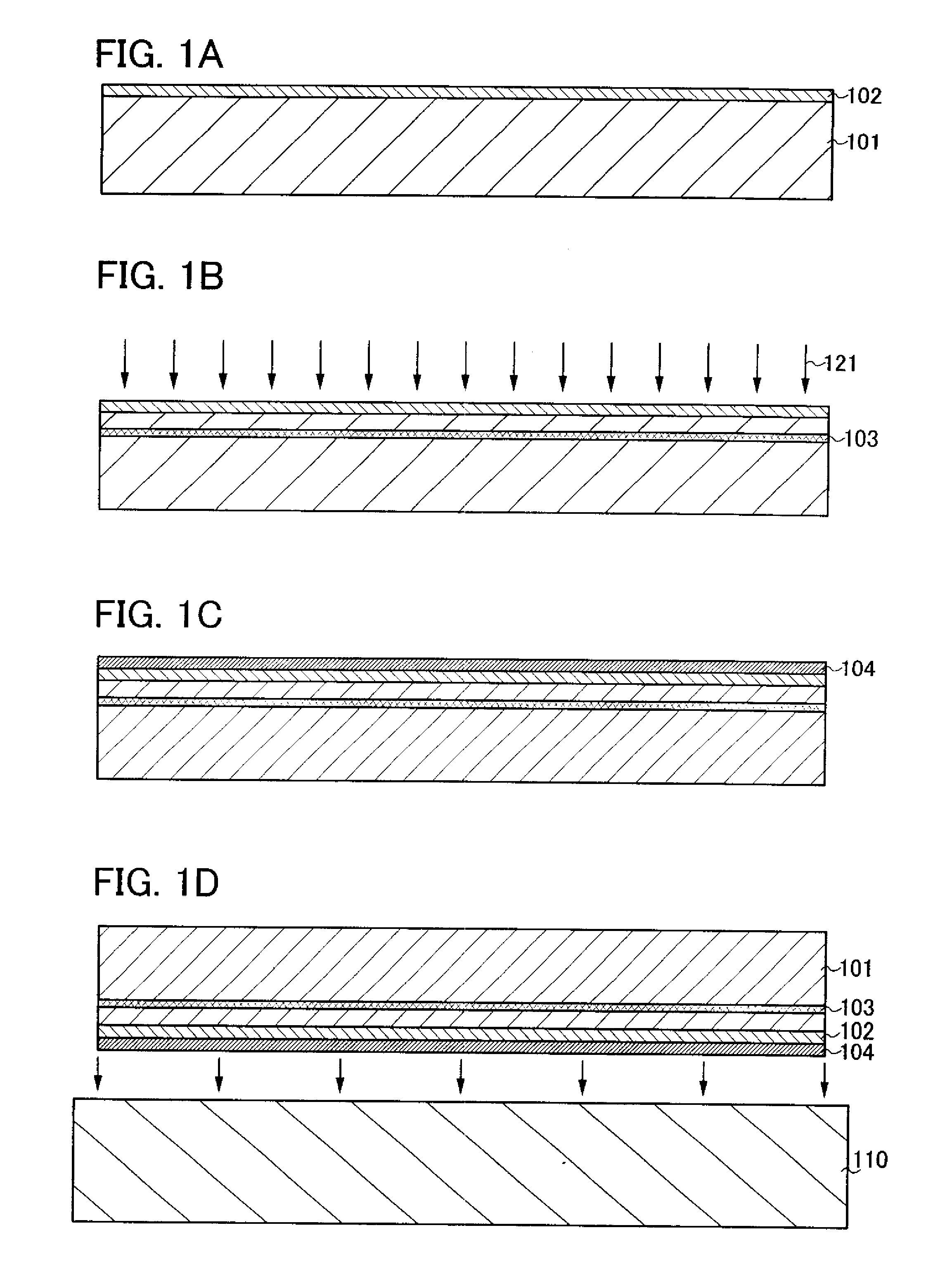
[0033]This embodiment mode describes an example of a method for manufacturing an SOI substrate with reference to the drawings.

[0034]First, a semiconductor substrate 101 is prepared, and an insulating layer 102 is formed on a surface of the semiconductor substrate 101 (see FIG. 1A).

[0035]As the semiconductor substrate 101, a commercial semiconductor substrate can be used; for example, a single-crystal silicon substrate, a single-crystal germanium substrate, and a compound semiconductor substrate of gallium arsenide, indium phosphide, or the like can be used. Typically, sizes of the commercial silicon substrates are 5 in. (125 mm), 6 in. (150 mm), 8 in. (200 mm), and 12 in. (300 mm) in diameter and shapes of the commercial silicon substrates are circular. Note that the shape of the commercial silicon substrate is not limited to the circular shape, and a silicon substrate which is processed into a rectangular shape or the like can be used.

[0036]An insulating layer having a smooth surfa...

embodiment mode 2

[0074]This embodiment mode describes a method for manufacturing an SOI substrate, which is different from that in the above-described embodiment mode, with reference to the drawings. Specifically, a manufacturing method in which a base substrate provided with a nitrogen-containing layer on a surface thereof and a semiconductor substrate are bonded to each other is described.

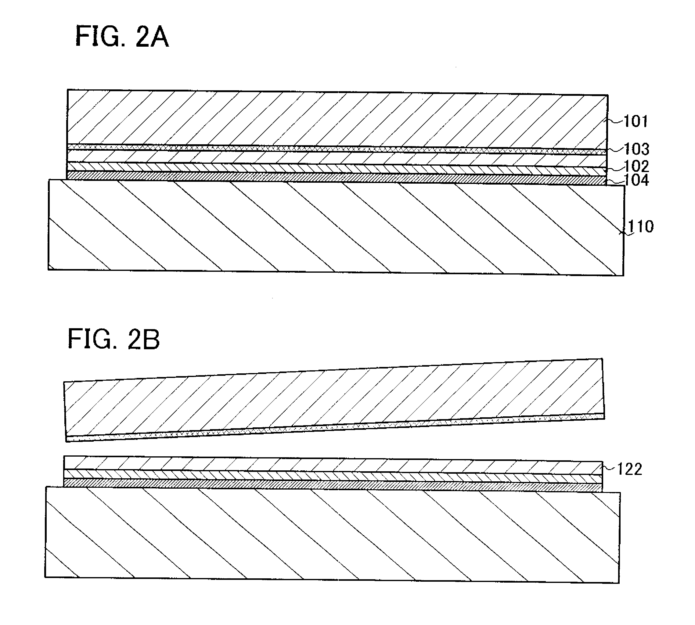
[0075]First, the semiconductor substrate 101 is prepared, and then an insulating layer 202 is formed on the surface of the semiconductor substrate 101 (see FIG. 3A).

[0076]In this embodiment mode, the insulating layer 202 which serves as a bonding layer to be bonded to the base substrate is provided on a surface where a bond is formed between the semiconductor substrate 101 and the base substrate. The insulating layer 202 may have a single layer structure or a stacked layer structure, and an insulating layer of which a surface to be bonded to the base substrate (hereinafter also referred to as a “bonding surface”)...

embodiment mode 3

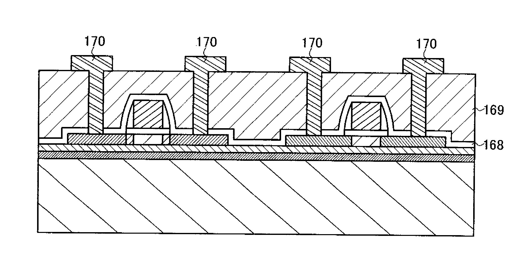
[0093]This embodiment mode describes a method for manufacturing a semiconductor device using the SOI substrate which is manufactured according to the above embodiment modes.

[0094]First, a method for manufacturing an n-channel transistor and a p-channel transistor is described as a method for manufacturing a semiconductor device with reference to FIGS. 5A to 5D and FIGS. 6A to 6C. By combining a plurality of thin film transistors (TFTs), various semiconductor devices can be formed.

[0095]In this embodiment mode, the SOI substrate which is manufactured according to the method of Embodiment Mode 1 is used as an SOI substrate. FIG. 5A is a cross-sectional view of the SOI substrate which is manufactured according to the method described with reference to FIGS. 1A to 1D.

[0096]The single-crystal semiconductor layer 122 of the SOI substrate is isolated for each element by etching, whereby a semiconductor layer 151 and a semiconductor layer 152 are formed as illustrated in FIG. 5B. The semico...


PUM


Abstract

An object of the present invention is to provide a method for manufacturing an SOI substrate provided with a semiconductor layer which can be used practically even where a substrate having a low upper temperature limit such as a glass substrate is used. The manufacturing method compromises the steps of preparing a semiconductor substrate provided with a bonding layer formed on a surface thereof and a separation layer formed at a predetermined depth from the surface thereof, bonding the bonding layer to the base substrate having a distortion point of 700° C. or lower so that the semiconductor substrate and the base substrate face each other, and separating a part of the semiconductor substrate at the separation layer by heat treatment in order to form a single-crystal semiconductor layer over the base substrate. In the manufacturing method, a substrate which shrinks isotropically at least by the heat treatment is used as the base substrate.

Description

BACKGROUND OF THE INVENTION[0001]1. Field of the Invention[0002]The present invention relates to an SOI (silicon on insulator) substrate. The present invention also relates to a semiconductor device manufactured using the SOI substrate.[0003]2. Description of the Related Art[0004]In recent years, integrated circuits using an SOI substrate where a thin single-crystal semiconductor layer is formed on an insulating surface, instead of a bulk silicon wafer, have been developed. Since parasitic capacitance between a drain of a transistor and a substrate is reduced by using the SOI substrate, the SOI substrate has been attracted attention as a substrate which improves performance of semiconductor integrated circuits.[0005]A Smart Cut (registered trademark) method is known as one of methods for manufacturing an SOI substrate (e.g., see Reference 1: Japanese Published Patent Application No. 2000-124092). An outline of a method for manufacturing an SOI substrate by a Smart Cut method is desc...

Claims


Application Information

Patent Timeline
IPC IPC(8): H01L21/31
CPCH01L21/2007H01L21/76254H01L29/66772H01L27/1266H01L27/1214H01L21/20H01L27/12
Inventor OHNUMA, HIDETOSHINGU, TAKASHIKAKEHATA, TETSUYAKURIKI, KAZUTAKAYAMAZAKI, SHUNPEI
Owner SEMICON ENERGY LAB CO LTD
Features
  • R&D
  • Intellectual Property
  • Life Sciences
  • Materials
  • Tech Scout
  • Unparalleled Data Quality
  • Higher Quality Content
  • 60% Fewer Hallucinations
Learn More