Dual gate fet structures for flexible gate array design methodologies

a flexible gate array and design methodology technology, applied in the direction of pulse technique, solid-state device, instruments, etc., can solve the problems of high cost, long design cycle and manufacturing time, and high cost of standard cell ic design errors

Inactive Publication Date: 2009-04-23
GLOBALFOUNDRIES INC
View PDF2 Cites 264 Cited by
  • Summary
  • Abstract
  • Description
  • Claims
  • Application Information

AI Technical Summary

Benefits of technology

[0014]A dual gate FET topology is disclosed for use in gate array background cell design and processes to implement design structures, wherein the channel region of a first gate and a second gate of the same device may be independently processed to produce asymmetric parametric responses, such that operating parameters, including threshold voltage, carrier concentration and drive strength for each gate may be optimized for particular circuit functions and applications. The dual gate-gate array structures may exhibit asymmetric performance characteristics with respect to each gate of the structure to accommodate system requirements or critical path timing constraints. The asymmetric channel regions may be used to construct circuit functions of multiple performance levels within the same physical area.

Problems solved by technology

A drawback to the standard cell design methodology is the requirement of longer design cycles and manufacturing times and therefore higher costs because all photolithographic mask levels of the integrated circuit (IC) are unique to a single design.
In addition, design errors within standard cell ICs can be expensive, requiring redesign of the IC from the transistor definition levels upward.
In this regard, gate array design cannot support a wide range of performance levels for a given circuit within the same chip floor plan area.
Transistor availability provided by the gate array background allows repair of the IC using only BEOL levels, reducing cost and time, however, because of limitations on performance and area associated with the gate array topology, repairs capable of fitting into available gate array background cells and meeting performance requirements may not be feasible.
This loss in efficiency is due both to the cell definition of two PFETs and two NFETs and to necessary isolation requirements between the source and drain diffusions within the gate array to implement the function.
As the schematic for the circuit grows, the physical implementation may grow at a rate faster than that of the schematic due to the need to tie certain transistors off to provide source / drain isolation, thus, the flexibility and efficiency of gate array circuits are severely limited.
Again, the size of these structures is quantized by strength-related parameters such as Vt, L and W of the FET in the gate array background—all of which limit design flexibility.

Method used


Image

  • Dual gate fet structures for flexible gate array design methodologies
  • Dual gate fet structures for flexible gate array design methodologies
  • Dual gate fet structures for flexible gate array design methodologies

Examples


Embodiment Construction

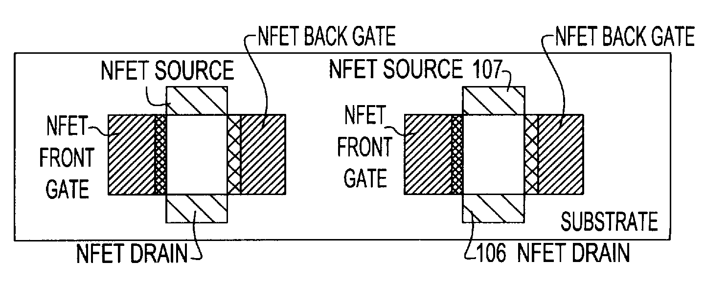
[0037]In a first aspect of the invention, a gate array cell utilizing dual gate NFET and PFET structures is presented. FIGS. 9a-c illustrate cross sections of a planar dual gate embodiment of the gate array cell which consists of two NFETs and two PFETs by example, but those skilled in the art will appreciate that many configurations with alternative FET counts are possible. The source and drain diffusion regions for the gate array cell are positioned at the far left and right of the cell in each of the PFET and NFET regions as well as in the center of the cell in the respective FET regions similar to prior art structures shown in FIGS. 1 and 2. However, the prior art surface channel FETs are replaced by dual gate FETs, which may be either symmetric or asymmetric in performance. The basic gate array cell structure is also differentiated from the prior art in that allocation is made for contacting of both the front and back gate of each transistor within the isolation regions of the ...


PUM


Abstract

A gate array cell adapted for standard cell design methodology or programmable gate array that incorporates a dual gate FET device to offer a range of performance options within the same unit cell area. The conductivity and drive strength of the dual gate device may be selectively tuned through independent processing of manufacturing parameters to provide an asymmetric circuit response for the device or a symmetric response as dictated by the circuit application.

Description

FIELD OF THE INVENTION[0001]The field of the invention is related to gate array circuit and design structures and methodologies, and more particularly to dual-gate FET structures with tunable performance characteristics for improved flexibility of embedded gate array circuit applications and topologies.BACKGROUND OF THE INVENTION[0002]Over the past two decades, two basic design styles have dominated the field of mask programmable Application Specific Integrated Circuit (ASIC) design: standard cell (SC) and Gate Array (GA). The standard cell methodology creates a library of primitive logic devices as well as higher level circuit functions to facilitate ease of design through the elimination of repetitive physical layout and verification for commonly used logic functions. Standard cell methodology offers circuit designers great flexibility in circuit tuning within the ASIC library as well as the option of placing multiple performance levels or drive strengths of a circuit within the s...

Claims


Application Information

Patent Timeline
Patent Type & Authority Applications(United States)
IPC IPC(8): H01L29/76H01L21/82G06F17/50
CPCH01L29/785H03K19/1778H01L29/78648
Inventor BARROWS, COREY K.IADANZA, JOSEPH A.NOWAK, EDWARD J.STOUT, DOUGLAS W.
Owner GLOBALFOUNDRIES INC
Why Eureka
Try Eureka