Semiconductor device, manufacturing method thereof, and data processing system

a technology of semiconductor devices and manufacturing methods, applied in the direction of semiconductor devices, basic electric elements, electrical appliances, etc., can solve the problems of deteriorating refresh characteristics, high leakage current of dram chips, and serious problems such as short channel effect, so as to improve threshold characteristics, reduce leakage current, and reduce the effect of dram leakage curren

Inactive Publication Date: 2009-04-23
LONGITUDE LICENSING LTD
View PDF1 Cites 8 Cited by
  • Summary
  • Abstract
  • Description
  • Claims
  • Application Information

AI Technical Summary

Benefits of technology

[0009]In this embodiment, it is preferable that a portion, in the active region, configuring the second bottom portion of the gate trench function as a main channel region, and the main channel region have a thin-film structure sandwiched between the gate electrode and the element isolation region. On the other hand, it is preferable that a portion, in the active region, configuring the first bottom portion of the gate trench function as a sub-channel region. In this case, preferably, a threshold voltage of the main channel region is lower than a threshold voltage of the sub-channel region. Further, preferably, the second bottom of the gate trench has an inversely arched side-wall. Thereby, the side-wall channel region is an extremely thin SOI structure, and when a gate-to-source voltage VGS is low, a current is passed to the side-wall channel region only, and when VGS is high, the current is passed to both the trench bottom and the side-wall channel region. Thus, a cut-off characteristic can be favorable, and a sub-threshold characteristic can be improved.
[0010]In this embodiment, it is preferable that a side-wall surface of the element isolation region have an upper-portion-side-wall surface approximately vertical to a semiconductor substrate and a lower-portion-side-wall surface having a tapered shape. In this case, preferably, the main channel region is arranged between the gate electrode and the lower-portion-side-wall surface of the element isolation region. When the side-wall surface of the element isolation region is thus shaped, the inversely arched channel region of the thin-film SOI structure can be surely formed, and thus the height of the side-wall channel region can be kept low.
[0014]According to the present invention, even in a fine transistor of which the gate width is equal to or less than 90 nm, for example, a curvature radius of the channel region can be made large. In this case, the effective channel length of the transistor becomes shorter than a groove gate. However, the channel region becomes an extremely thin SOI structure, and a cut-off characteristic becomes preferable. Thus, a threshold characteristic can be improved. As a result, a leakage current can be suppressed, and when the structure is applied to the memory cell transistor of the DRAM, a refresh characteristic can be enhanced.

Problems solved by technology

The short gate length of the transistor leads to short channel effect degradation which results in high leakage current of a DRAM chip.
Thus, the DRAM is confronted with the serious problem of this short channel effect.
As a result, there is a problem that when the width of the gate trench is narrower, the refresh characteristic deteriorates.

Method used


Image

  • Semiconductor device, manufacturing method thereof, and data processing system
  • Semiconductor device, manufacturing method thereof, and data processing system
  • Semiconductor device, manufacturing method thereof, and data processing system

Examples


Embodiment Construction

[0031]Preferred embodiments of the present invention will now be explained in detail with reference to the drawings.

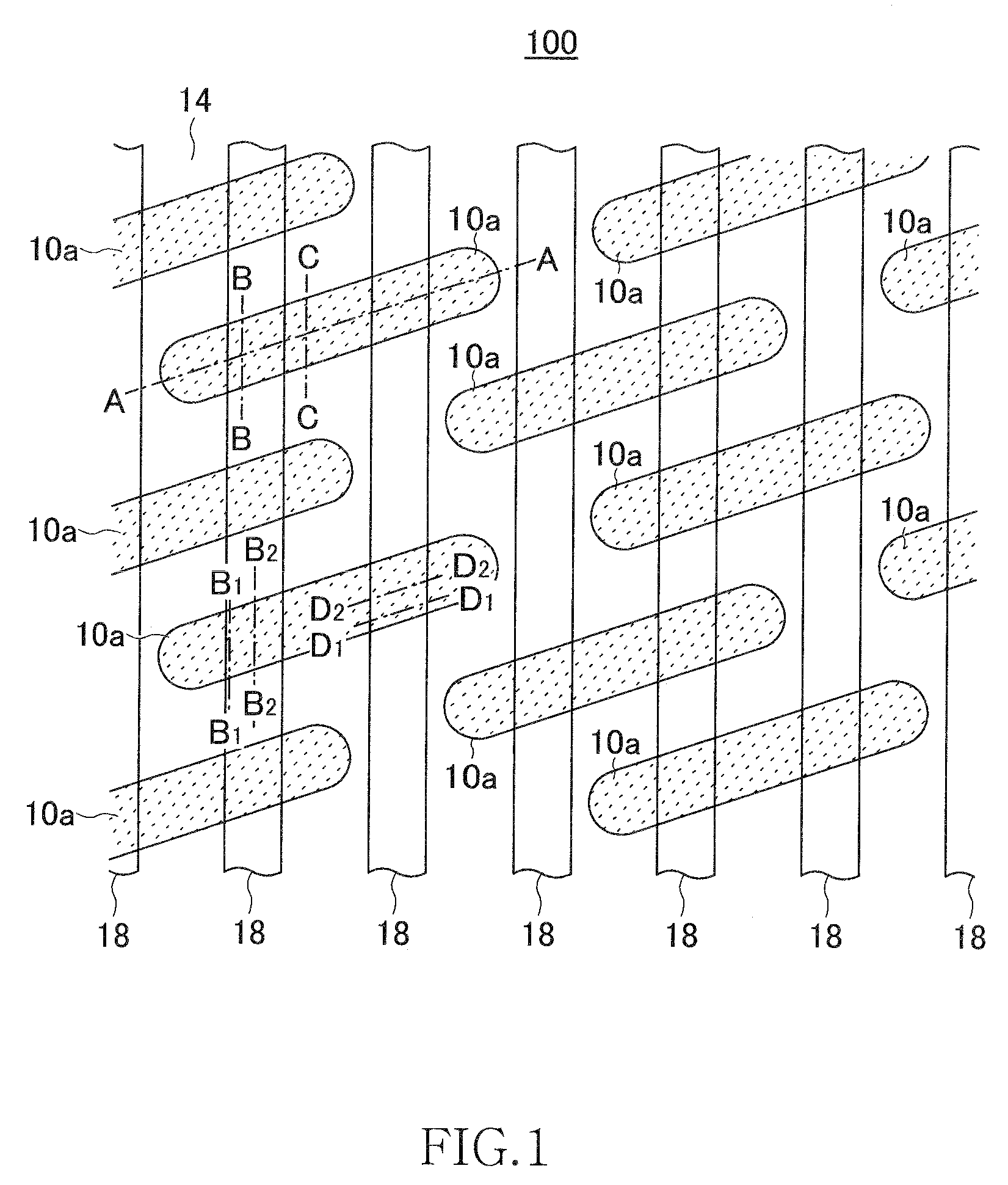
[0032]FIG. 1 is a schematic plan view showing a layout of a main part of a semiconductor device according to an embodiment of the present invention.

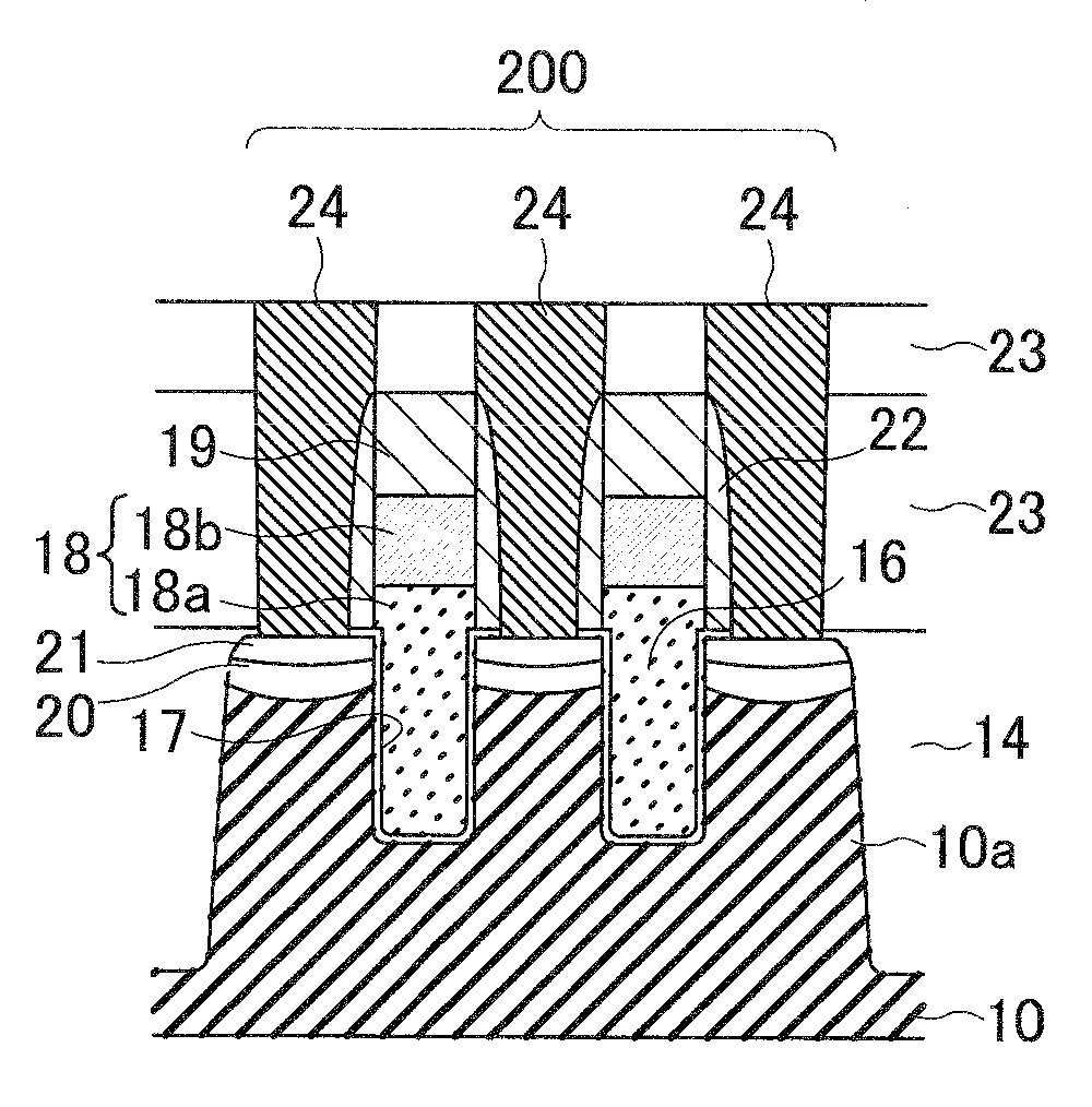
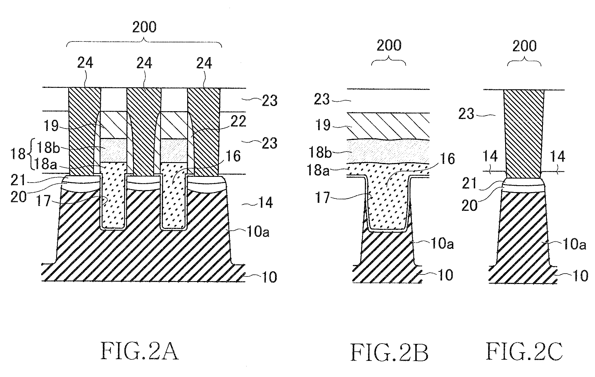
[0033]A semiconductor device 100 according to the present embodiment is a memory cell of a DRAM, and includes a plurality of active regions 10a formed therein with cell transistors and a plurality of gate electrodes 18 formed in one direction extending across the active regions 10a, as shown in FIG. 1. Although not shown in FIG. 1, the memory cell of the DRAM is formed of one cell transistor and one cell capacitor, and has a structure in which cell capacitors are stacked vertically one after another above the cell transistor formed within the active regions 10a. The active regions 10a have an elongated planar shape of which the periphery is surrounded by STI (Shallow Trench Isolation) 14, and a longitudinal direction of the...


PUM


Abstract

A bottom of a gate trench has a first bottom relatively far from an STI and a second bottom relatively near from the STI A portion, in an active region, configuring the second bottom of the gate trench configures a side-wall channel region, and has a thin-film SOI structure sandwiched between the gate electrode and the STI. On the other hand, a portion configuring the first bottom of the gate trench functions as a sub-channel region. A curvature radius of the second bottom is larger than a curvature radius of the first bottom. In an approximate center in a width direction of the gate trench, a bottom of a trench is approximately flat, and on the other hand, in ends of the width direction, a nearly whole bottom of the trench is curved.

Description

BACKGROUND OF THE INVENTION[0001]1. Field of the Invention[0002]The present invention relates to a semiconductor device and a manufacturing method thereof, and, more particularly relates to a semiconductor device including a trench-gate transistor and a manufacturing method thereof. The present invention also relates to a data processing system configured by such a semiconductor device.[0003]2. Description of Related Art[0004]In recent years, downscaling of high density and lower power DRAM (Dynamic Random Access Memory) requires a very short gate length of a cell transistor. The short gate length of the transistor leads to short channel effect degradation which results in high leakage current of a DRAM chip. Thus, the DRAM is confronted with the serious problem of this short channel effect.[0005]To overcome this problem, attention is paid to a so-called trench-gate transistor (also called a “recess-channel transistor”) so configured that a gate electrode is buried in a groove (tren...

Claims


Application Information

Patent Timeline
Patent Type & Authority Applications(United States)
IPC IPC(8): H01L29/78H01L21/3205
CPCH01L27/10876H01L29/66621H01L29/4933H01L29/4236H10B12/053
Inventor KUJIRAI, HIROSHI
Owner LONGITUDE LICENSING LTD
Why Eureka
Try Eureka