Delay adjusting method and LSI that uses air-gap wiring

a delay adjustment and air gap technology, applied in the field of optimizing technology of semiconductor integrated circuit devices, can solve the problems of increasing the parametric capacitance between adjacent wirings, wasting wiring channels, and complicated manufacturing process, and achieves the effect of suppressing the addition of manufacturing process, without increasing cost and ta

Active Publication Date: 2009-04-23
KOKUSA ELECTRIC CO LTD
View PDF8 Cites 5 Cited by
  • Summary
  • Abstract
  • Description
  • Claims
  • Application Information

AI Technical Summary

Benefits of technology

[0010]The present invention has been made to dissolve the above-mentioned conventional problems. An object of the present invention is, on the premise of an application of the Air-Gap technology, to provide a method for manufacturing a semiconductor integrated circuit device capable of timing optimization with suppressing additions to the manufacturing process and without increase in cost and TAT.

Problems solved by technology

For this reason, in the case where the Air-Gap technology is applied to the above-mentioned conventional art 1, when the distance between adjacent wirings is made larger than the specified spacing, no void (Air-Gap) will come to exist there, and a problem arises that a parasitic capacitance between adjacent wirings will be increased conversely unlike the conventional art 1.
Delay adjustment by means of a wiring load of the above-mentioned conventional art 1 in a range within the specified wiring spacing in which the void (Air-Gap) is formed, since a wiring pitch dependability becomes extremely small, redrawing of wirings is required over the longer wiring length, and gives rise to the problem of wasting wiring channels.
Further, since the above-mentioned conventional art 2 is a technology to add a new special insulating material in addition to an insulating material used usually to the insulating film between wiring layers, a manufacturing process becomes complicated, and additional equipment is needed to be secured to an existing manufacturing line, and an application of new materials will give rise to a problem that cost and TAT are increased including a securement of reliability.

Method used


Image

  • Delay adjusting method and LSI that uses air-gap wiring
  • Delay adjusting method and LSI that uses air-gap wiring
  • Delay adjusting method and LSI that uses air-gap wiring

Examples


Embodiment Construction

[0029]Hereinafter, embodiments of the present invention will be described in detail with reference to the accompanying drawings. Note that, components having the same function are denoted by the same reference symbols throughout the drawings for describing the embodiment, and the repetitive description thereof will be omitted.

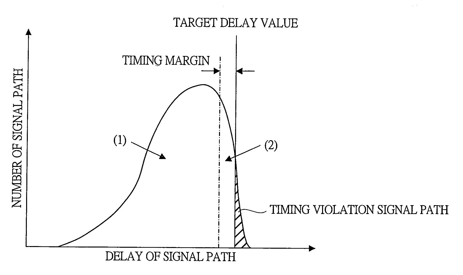
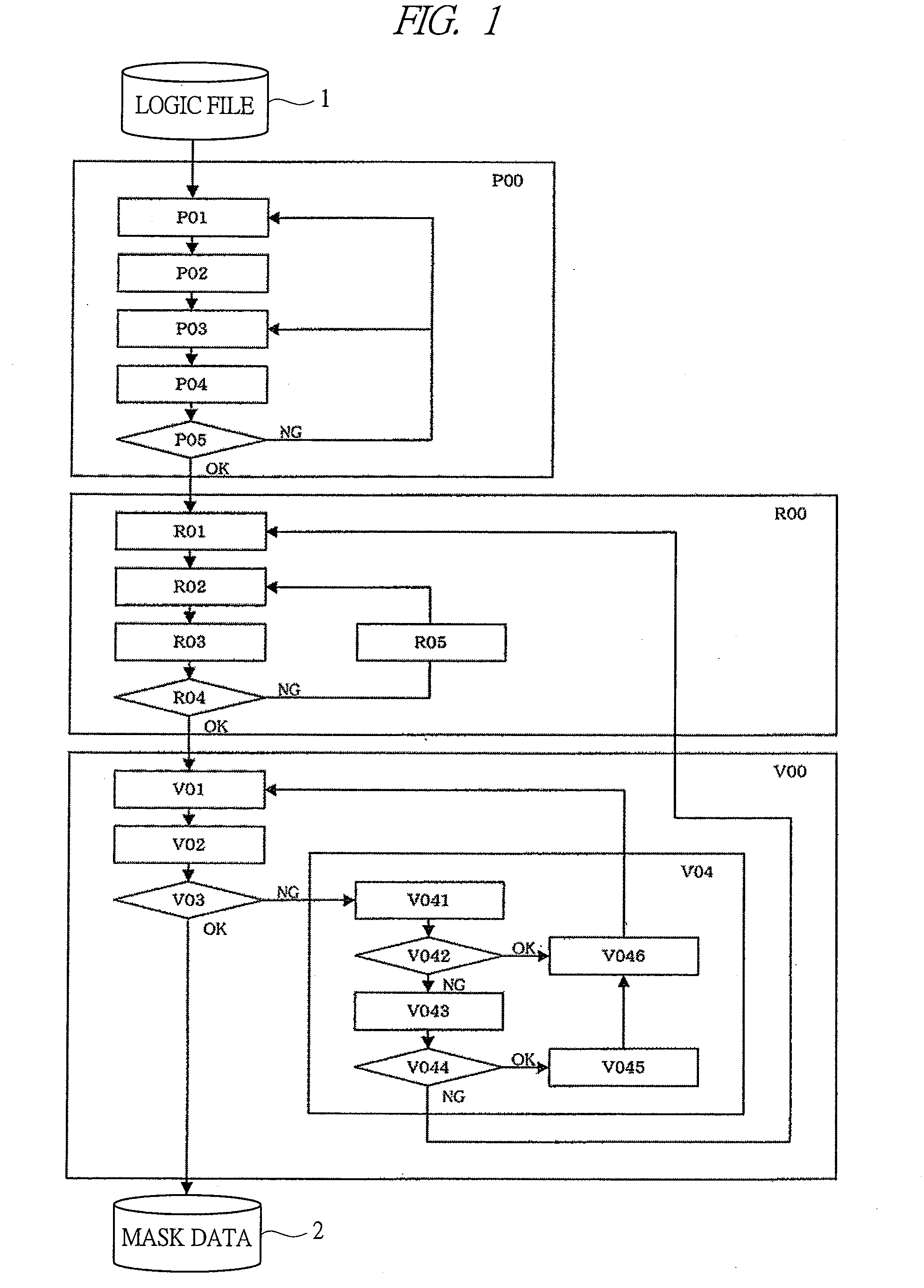
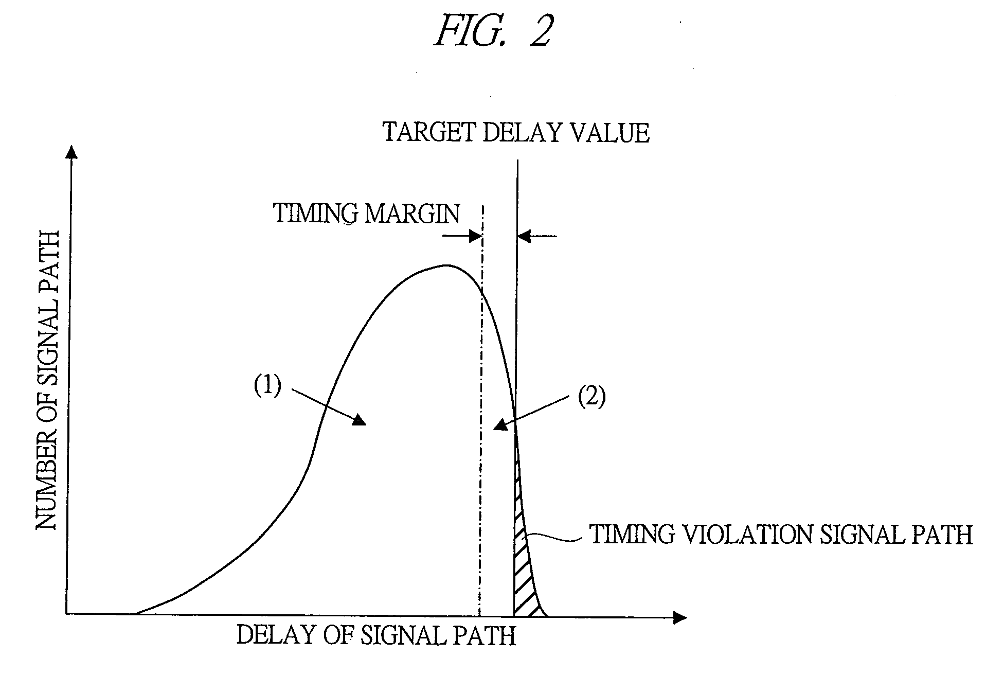
[0030]FIG. 1 is a flowchart of a layout design level in a manufacturing method of a semiconductor integrated circuit device according to an embodiment of the present invention. A circuit design is performed in advance of the layout design, and the circuit design information is stored in a logic file 1.

[0031]The layout design includes a placing step P00 for determining a position arrangement of a logic block, a flip-flop, a buffer, etc., a routing step R00 for determining a layout of wiring, and a verification step V00 for confirming a final operation speed.

[0032]The placing step P00 includes: a cell placing step P01 for arranging a logic cell (a logic block and...


PUM


Abstract

Provided is a method for manufacturing a semiconductor integrated circuit device which enables a timing optimization without giving additions to a manufacturing process and increasing cost and TAT. Existence of a timing constraint violation is determined, and when a timing constraint violation is detected, to dissolve the violation, a void formation inhibition zone is set up in a part or all of a spacing (inter-wiring spacing) between an optimization-target wiring which needs a further delay time of a signal and clock and an adjacent wiring adjacent to the optimization-target wiring having a spacing within a specified wiring spacing, and an insulating film is formed in a spacing (inter-wiring spacing) between the optimization-target wiring and the adjacent wiring in the void formation inhibition zone, and voids are formed in a spacing (inter-wiring spacing) between the optimization-target wiring and the adjacent wiring outside the void formation inhibition zone.

Description

CROSS-REFERENCE TO RELATED APPLICATION[0001]The present application claims priority from Japanese Patent Application No. JP 2007-270820 filed on Oct. 18, 2007, the content of which is hereby incorporated by reference into this application.TECHNICAL FIELD OF THE INVENTION[0002]The present invention relates to a manufacturing method of a semiconductor integrated circuit device. More particularly, the present invention relates to an optimization technology of the semiconductor integrated circuit device for complying with design constraints of delay time.BACKGROUND OF THE INVENTION[0003]Timing optimization is carried out here and there in the design process of semiconductor integrated circuit devices. Conventionally, corrections at RTL (Resistor-Transistor Level), addition of a logic cell, and replacement of a logic cell etc. have been performed. Addition and replacement of logic cells aims to adjust a speed of charging and discharging of a load by size changes of a transistor or by thr...

Claims


Application Information

Patent Timeline
Patent Type & Authority Applications(United States)
IPC IPC(8): G06F17/50
CPCG06F17/5031H01L21/7682H01L2924/0002H01L2924/00G06F30/3312
Inventor MATSUMOTO, TAKASHINOGUCHI, JUNJIOSHIMA, TAKAYUKI
Owner KOKUSA ELECTRIC CO LTD
Why Eureka
Try Eureka