High Efficiency Dilute Nitride Light Emitting Diodes

a light-emitting diode, high-efficiency technology, applied in the direction of semiconductor/solid-state device manufacturing, electrical apparatus, semiconductor devices, etc., can solve the problems of low internal quantum efficiency, poor temperature stability, yellow-red alingap-based light-emitting devices, etc., to achieve better temperature stability, reduce the shift of emitted wavelength, and improve luminescence efficiency

Inactive Publication Date: 2009-04-30
RGT UNIV OF CALIFORNIA
View PDF6 Cites 28 Cited by
  • Summary
  • Abstract
  • Description
  • Claims
  • Application Information

AI Technical Summary

Benefits of technology

[0013]One set of embodiments of the invention includes an LED structure comprising one or a plurality of active layers that comprise at least one element selected from the group consisting of Al, In, and Ga; N in a concentration range from about 0.001≦[N]≦0.1, preferably in the range from about 0.004≦[N]≦0.02; and at least one element selected from the group consisting of As, Sb, and P. The one or more active layers may be interleaved with a plurality of barrier layers comprising AlnGa1-nP where 0≦n≦1. The bandgap of the barrier layers may be larger than that of the active layer. The larger bandgap of the barrier layers may aid in confinement of electrical carriers (holes and electrons) in the active layer.
[0014]The plurality of active layers interleaved with the plurality of barrier layers as a whole are referred to as an active region that emits light. In a specific embodiment of the invention, the one or more active layers may have a higher luminescence efficiency and a smaller shift in emitted wavelength, as well as better temperature stability, than a LED formed from the conventional AlInGaP material system.

Problems solved by technology

There are a number of known difficulties with currently used yellow-red AlInGaP-based light emitting devices.
For example, they suffer from low internal quantum efficiency and poor temperature stability in the yellow-red range, which is usually attributed to poor electron confinement.
In addition, the conventional procedure for removing the light absorbing GaAs substrate and wafer bonding a transparent substrate or reflective layer to the formed layer has a low yield and adds several relatively expensive processing steps, thus resulting in high costs.

Method used


Image

  • High Efficiency Dilute Nitride Light Emitting Diodes
  • High Efficiency Dilute Nitride Light Emitting Diodes
  • High Efficiency Dilute Nitride Light Emitting Diodes

Examples


Embodiment Construction

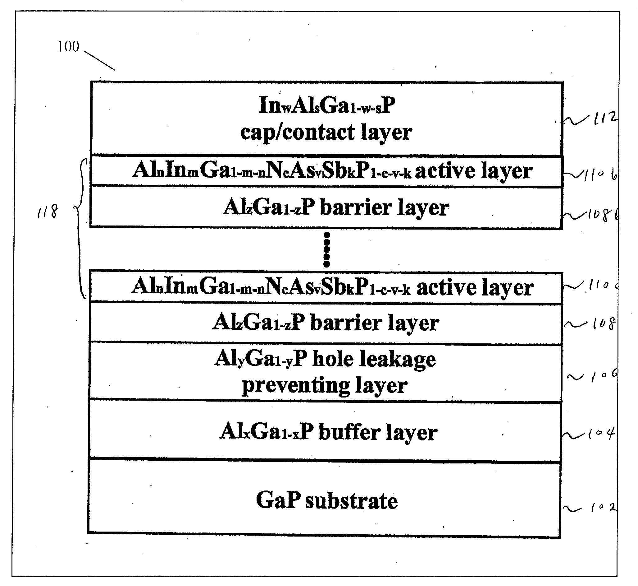
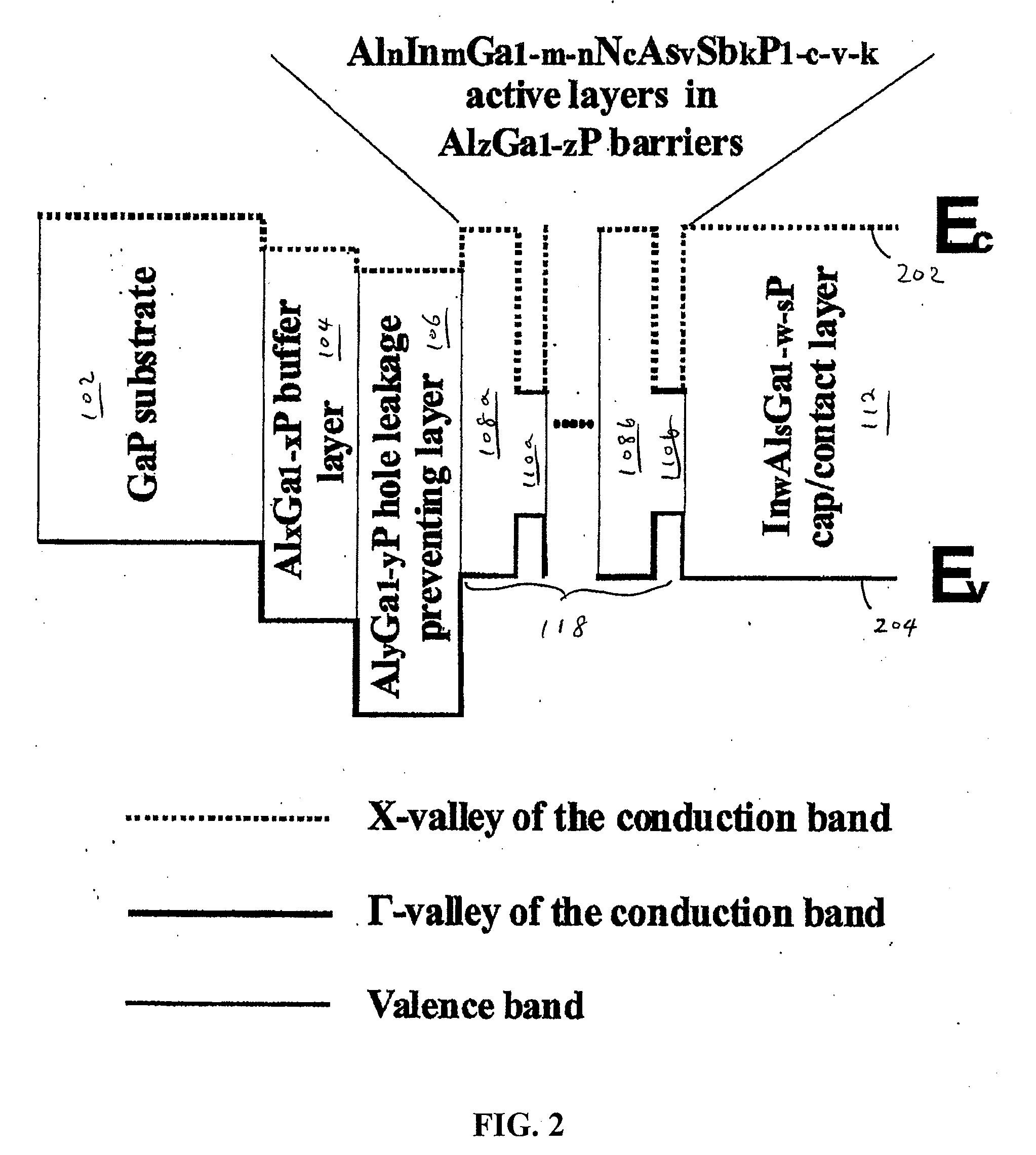
[0035]FIG. 1 shows an exemplary LED structure 100 of the present invention. The LED structure comprises a substrate 102, a buffer layer 104, a hole-leakage-prevention layer 106, a plurality of barrier layers 108, a plurality of active layers 110 and a cap / contact layer 112. FIG. 2 shows a schematic of one of the possible band diagrams for the LED structure 100 shown in FIG. 1. Ec is the conduction band minimum, while Ev is the valence band maximum.

[0036]Substrate 102 may comprise GaP or silicon, however this is not a limitation of the present invention and in other embodiments other substrates may be used, such as sapphire, AlN, plastic, quartz, glass, metal, etc.

[0037]Buffer layer 104 may comprise AlxGa1-xP where 0≦x≦1 and be formed over a substrate 102. Buffer layer 104 may be useful to obtain a smooth surface on substrate 102 for subsequent growth of the layers comprising LED structure 100. In some embodiments buffer layer 104 may be undoped or doped n-type or p-type. In some emb...


PUM


Abstract

A light-emitting diode comprising AlnInmGa1-m-nNcAsvSbkP1-c-v-k where 0.001<c<0.1 and 0≦n, m, v, k≦1 adapted to emit light in a wavelength range of about 540 nm to about 700 nm.

Description

CROSS-REFERENCES TO RELATED APPLICATIONS[0001]This patent application is a continuation-in-part of U.S. patent application Ser. No. 11 / 576,992, entitled “HIGH EFFICIENCY LIGHT-EMITTING DIODES,” filed Apr. 10, 2007, which is a U.S. national phase application of International Application No. PCT / US2005 / 036538, entitled “HIGH EFFICIENCY LIGHT-EMITTING DIODES,” filed Oct. 8, 2005, which is a patent application under the Paris Convention Treaty of U.S. Provisional Patent Application No. 60 / 617,465, entitled “HIGH EFFICIENCY LED'S AND LASERS,” filed Oct. 8, 2004. The disclosures of these three applications are hereby incorporated by reference in their entirety for all purposes.BACKGROUND OF THE INVENTION[0002]This application relates to high efficiency light-emitting diodes directly grown over transparent GaP substrates.[0003]Solid-state lighting with light emitting diodes (LEDs) has become one of the most exciting subjects in research and business. Applications for these LEDs include ful...

Claims


Application Information

Patent Timeline
Patent Type & Authority Applications(United States)
IPC IPC(8): H01L33/00H01L21/02H01L33/02H01L33/12H01L33/32
CPCH01L21/02392H01L21/02461H01L21/02543H01L33/32H01L33/0095H01L33/025H01L33/12H01L33/0075
Inventor TU, CHARLESODNOBLYUDOV, VLADIMIR
Owner RGT UNIV OF CALIFORNIA
Why Eureka
Try Eureka