Semiconductor device and its fabrication process

a technology of semiconductor devices and fabrication processes, applied in semiconductor devices, semiconductor/solid-state device details, electrical apparatus, etc., can solve the problems of generating whiskers, short-circuit malfunction of semiconductor devices, and forming needle-like crystals, so as to prevent the generation of whiskers caused by compressive stress and the effect of compressive stress

Inactive Publication Date: 2009-04-30
RENESAS ELECTRONICS CORP
View PDF8 Cites 13 Cited by
  • Summary
  • Abstract
  • Description
  • Claims
  • Application Information

AI Technical Summary

Benefits of technology

[0005]The leads of the semiconductor device and terminals of the mounting board are connected, for example, by using solder. At this point, generally, plating films are formed on the surfaces of the leads to improve the wettability of the leads and the solder or to prevent corrosion or oxidation of the leads because the primary material of the leads is generally copper. From the viewpoint of realization of this objective and from the viewpoint of cost reduction, a film containing tin as a primary material is used as the plating film.
[0009]The whiskers are generated in the plating film due to the compressive stress generated by the abovedescribed causes. In conventional techniques, in order to prevent the whiskers generated in the plating film containing tin as a primary material, lead (Pb) elements has been introduced into the plating film. Although the detailed mechanism thereof is unknown, generation of whiskers in the plating film can be prevented by adding lead to the plating film containing tin as a primary material.
[0011]An object of the present invention is to provide a technique capable of preventing whiskers generated in a plating film that is formed on a surface of a lead of a semiconductor device. More particularly, an object of the present invention is to provide a technique capable of preventing generation of whiskers in a plating film containing tin as a primary material and not containing lead.
[0015]Consequently, the coefficient of thermal expansion in a surface of the plating film becomes smaller than the coefficient of thermal expansion of the copper (lead); thus, even when thermal load by repetitive application of high temperatures and low temperatures is applied, compressive stress can be prevented from acting on the surface of the plating film when it is put at a high temperature. That is, since the coefficient of thermal expansion in the surface of the plating film is smaller than the coefficient of thermal expansion of the copper, the plating film is pulled by the lead containing copper as a primary material. Thus, tensile stress acts on the plating film instead of compressive stress; therefore, generation of whiskers caused by compressive stress can be prevented.
[0017]Consequently, tensile stress acts on the plating film instead of compressive stress when it is put at a high temperature; therefore, generation of whiskers caused by compressive stress can be prevented.
[0019]The coefficient of thermal expansion in the surface of the plating film is smaller than the coefficient of thermal expansion of copper; therefore, generation of whiskers caused by compressive stress can be prevented.

Problems solved by technology

However, in the plating film containing tin as a primary material, formation of needle-like crystals called whiskers has been a problem.
This means that short-circuit malfunction occurs in the semiconductor device since the adjacent leads are electrically connected to each other by the whiskers.
More specifically, it is conceived that, when compressive stress is applied to the plating film, part of the plating film that cannot withstand the compressive stress any more projects, thereby generating whiskers.

Method used


Image

  • Semiconductor device and its fabrication process
  • Semiconductor device and its fabrication process
  • Semiconductor device and its fabrication process

Examples


first embodiment

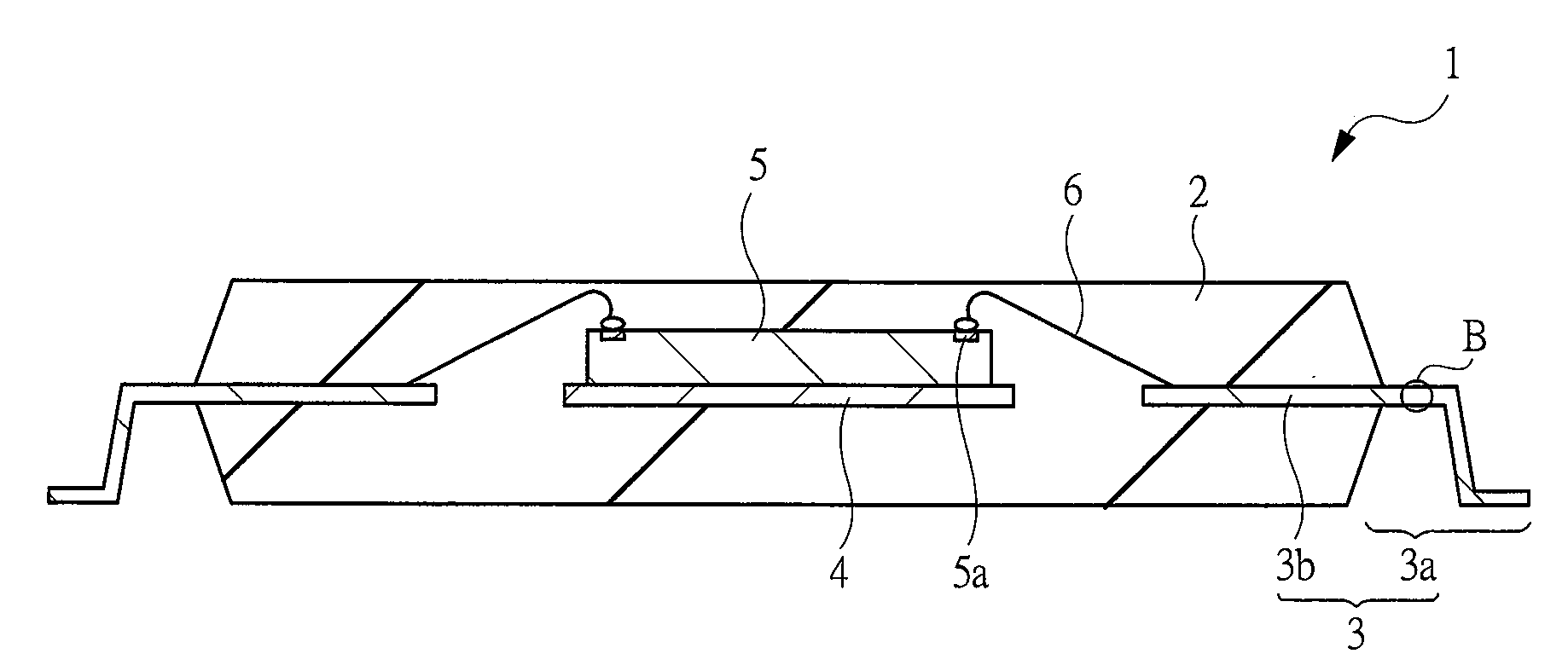
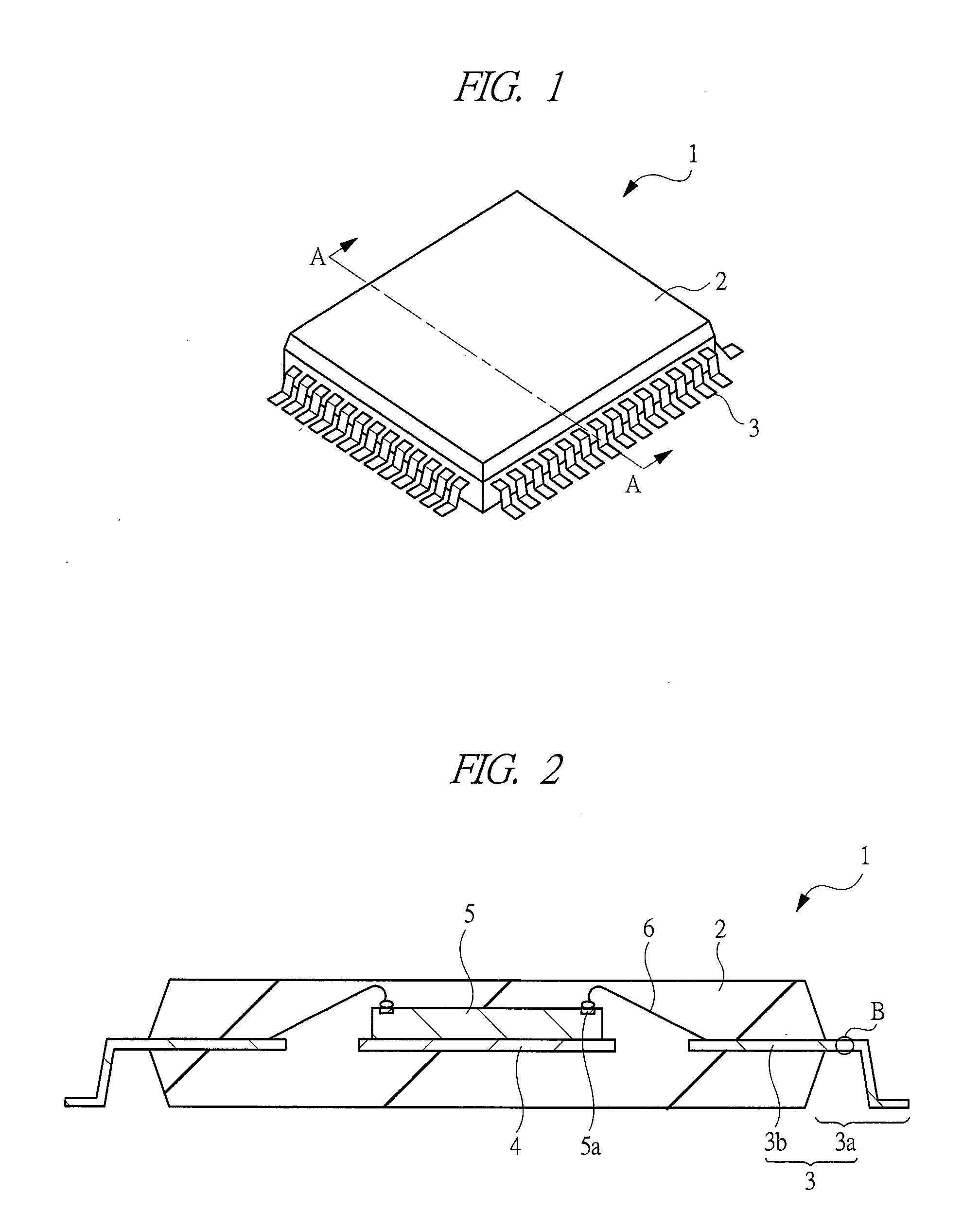
[0048]FIG. 1 is a perspective view showing an external appearance of a semiconductor device according to a first embodiment. The package configuration of the semiconductor device according to the first embodiment is a QFP (Quad Flat Package). As shown in FIG. 1, the semiconductor device 1 according to the first embodiment is covered by a resin (sealant) 2 having a shape of a rectangular parallelepiped, and leads 3 are projecting from four side surfaces of the resin 2. The lead 3 has a structure bent in an L shape.

[0049]FIG. 2 is a cross-sectional view showing a cross section taken along the line A-A of FIG. 1. As shown in FIG. 2, the lead 3 comprises an outer lead 3a projecting from the side surface of the resin 2 and an inner lead 3b formed in the inside of the resin 2. A tab 4 is formed at a center part sandwiched by the inner leads 3b at the left and the right (surrounded by the plurality of inner leads 3b), and a semiconductor chip 5 is disposed on the tab 4. On the semiconducto...

second embodiment

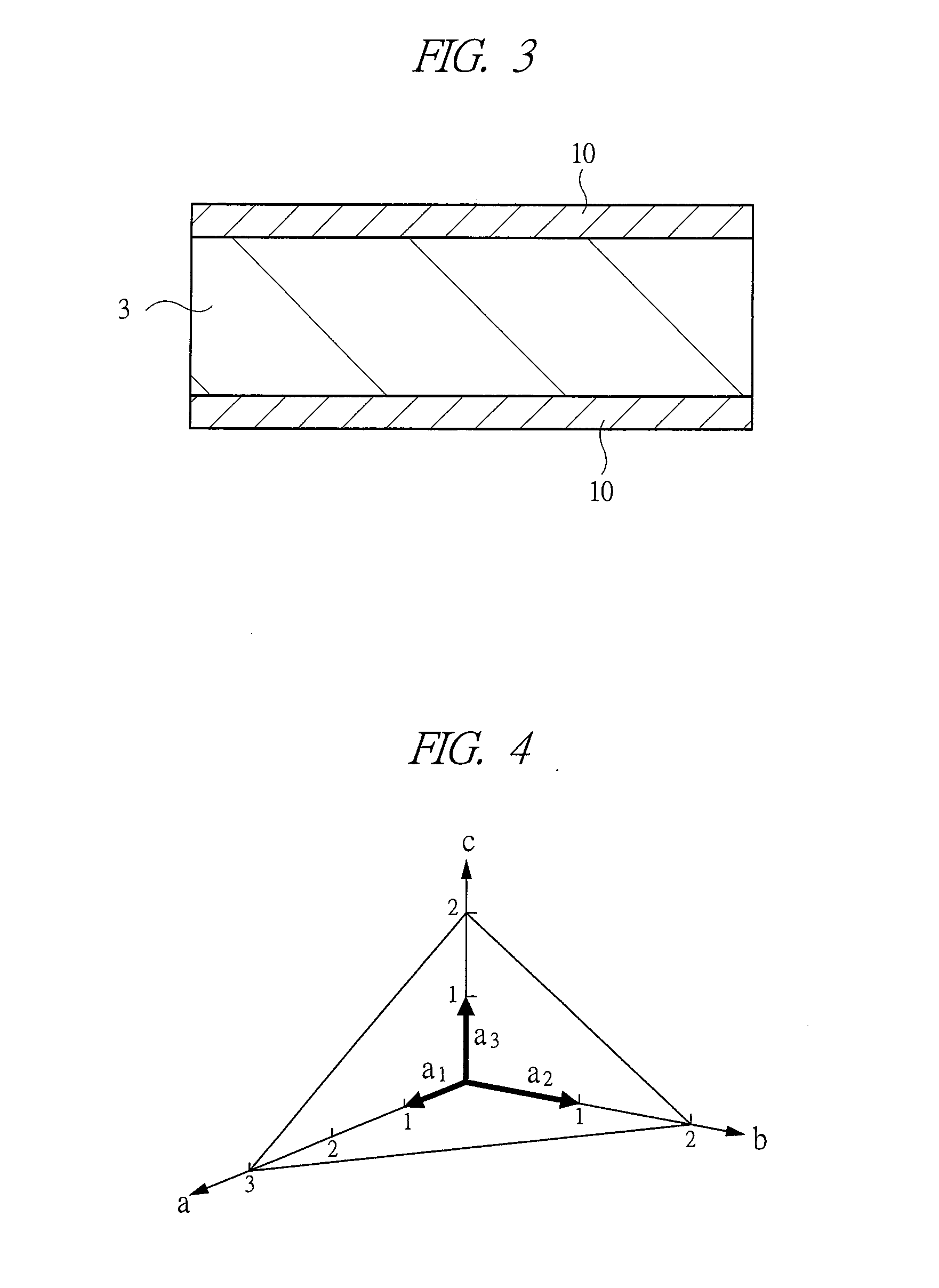
[0093]In a second embodiment, an example in which a plating film formed on a surface of a lead has a multi-layered structure will be described. FIG. 22 is a cross-sectional view showing a constitution of the plating film formed on the lead 3 in a semiconductor device according to the second embodiment. In FIG. 22, the gold film 11 is formed on the surface of the lead 3, and the plating film 10 containing tin as a primary material is formed on the gold film 11. The plating film 10 serves as a first plating layer, and a plating film 15 containing tin as a primary material is further formed on the plating film 10. In this manner, in the second embodiment, the multilayered film comprising the plating film 10 and the plating film 15 is formed on the gold film 11.

[0094]Herein, the gold film 11 has a function of controlling the crystal plane (plane orientation) of the plating film 10 formed on the gold film 11 to be in a particular direction. Specifically, as described in the abovedescribe...


PUM

PropertyMeasurementUnit
coefficient of thermal expansionaaaaaaaaaa
coefficients of thermal expansionaaaaaaaaaa
crystal structureaaaaaaaaaa

Abstract

A technique capable of preventing whiskers which are generated in a plating film formed on the surface of each of leads of a semiconductor device is provided. Particularly, a technique capable of preventing generation of whiskers in a plating film containing tin as a primary material and not containing lead is provided. The plating film formed on the surface of the lead is formed so that a particular plane orientation among plane orientations of tin constituting the plating film is parallel to the surface of the lead. Specifically, the plating film is formed so that the (001) plane of tin is parallel to the surface of the lead. Thus, the coefficient of thermal expansion of tin constituting the plating film can be made to be lower than a coefficient of thermal expansion of the copper constituting the lead.

Description

CROSS-REFERENCE TO RELATED APPLICATION[0001]The present application claims priority from Japanese Patent Application No. JP 2007-278437 filed on Oct. 26, 2007, the content of which is hereby incorporated by reference into this application.TECHNICAL FIELD OF THE INVENTION[0002]The present invention relates to a semiconductor device and its fabrication process. More particularly, the present invention relates to a technique effectively applied to a semiconductor device using a plating film containing tin (Sn) as a primary material and not containing lead (Pb), and to fabrication of the same.BACKGROUND OF THE INVENTION[0003]IEEE TRANSACTIONS ON ELECTRONICS PACKAGING MANUFACTURING, pp 265-273, VOL. 29, NO. 4, OCTOBER 2006 (Non-Patent Document 1) describes a review about needle-like crystals (whiskers) generated in a plating film containing tin as a primary component and not containing lead. In this review, growth of whiskers generated in tin is discussed on the basis of stress (strain e...

Claims


Application Information

Patent Timeline
Patent Type & Authority Applications(United States)
IPC IPC(8): H01L23/495H01L21/00
CPCH01L23/49582H01L2224/48247H01L2224/78301H01L2924/01078H01L2924/01079H01L24/48H01L2924/1306H01L2924/01019H01L24/97H01L2924/00H01L2224/45139H01L2924/181H01L2224/45144H01L2924/14H01L2924/00014H01L2224/48465H01L2924/00011H01L2924/00012H01L2224/45099H01L2224/45015H01L2924/207H01L2924/01049H01L2924/01005H01L23/48
Inventor OKURA, YASUTAKAIWASAKI, TOMIOTERASAKI, TAKESHI
Owner RENESAS ELECTRONICS CORP
Why Eureka
Try Eureka