Liquid crystal optical device manufacturing process

a manufacturing process and liquid crystal technology, applied in non-linear optics, instruments, optics, etc., can solve the problems of low durability, low production efficiency, and high cost, and achieve high deposition rate, excellent durability, and uniform manufacturing over a large area

Inactive Publication Date: 2009-04-30
CANON KK
View PDF32 Cites 9 Cited by
  • Summary
  • Abstract
  • Description
  • Claims
  • Application Information

AI Technical Summary

Benefits of technology

[0019]According to the process of the present invention, a liquid crystal alignment film formed of an inorganic material having excellent durability can be manufactured uniformly over a large area and at a high deposition rate.

Problems solved by technology

However, in liquid crystal display devices used as light shutters of projection type displays, the liquid crystal is exposed to strong light, and hence the high-molecular film tends to deteriorate and can not be expected to have a high durability.
Even in a polyimide alignment film which is chemically more stable than other polymer molecules, its chemical structure is broken down due to exposure to strong light and it cannot withstand long-time service.
The inclination angle and azimuth angle of the columns directly determine the alignment of liquid crystal molecules, and hence their non-uniformity brings about substrate in-plane alignment non-uniformity.
In this case, since the deposition angle should be constant in individual devices, non-uniformity over the whole substrate may be tolerable to a certain extent.
However, when two substrate with an alignment film formed therebetween are joined together, there are difficulties such that characteristics are not uniform between liquid crystal display devices which have been divided, because the differences in deposition angles between the upper and lower alignment film occur in the vicinity of the substrate ends and such differences are changed depending on positions.
Such non-uniform characteristics may result in such an inconvenience that when used as light valves of projection type displays, the optical axes and electrical responses of the light valves differ for each device, and projection optical systems must be adjusted for individual devices.

Method used


Image

  • Liquid crystal optical device manufacturing process
  • Liquid crystal optical device manufacturing process
  • Liquid crystal optical device manufacturing process

Examples


example 1

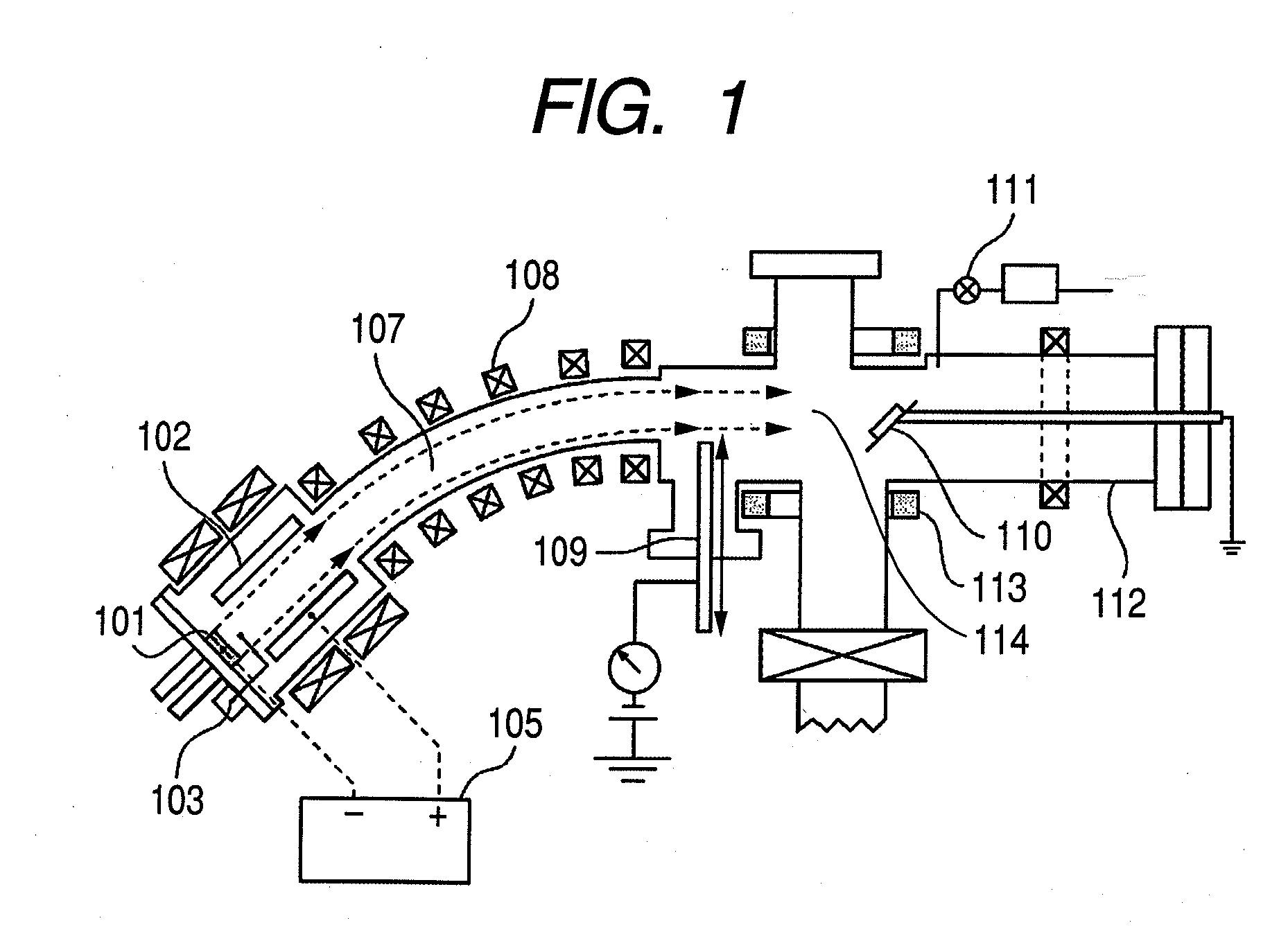
[0100]An inorganic alignment film was formed on glass substrates by means of the vacuum arc plasma film forming system shown in FIG. 1.

[0101]An alloy of 92% of silicon and 8% of aluminum was used as a material for the cathode 101. Oxygen gas was fed into the film forming chamber 114 to form an inorganic alignment film composed of Al2O3 and SiO2.

[0102]The substrate used was an alkali-free glass substrate of 0.7 mm in thickness. On the surface of the substrate, an ITO film was formed in a thickness of 20 nm. This substrate was cut in a size of 20 mm square to prepare film-formed glass substrates 510.

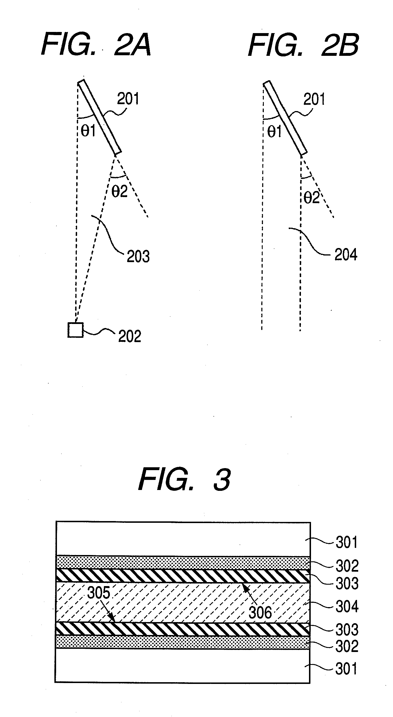
[0103]The arrangement of the glass substrates 510 at the time the alignment film was formed is shown in FIGS. 5A and 5B. Nine sheets of the film-formed glass substrates 510 were arranged as shown therein and were held in a substrate holder 503. This holder with substrates was set in the vacuum arc plasma film forming system shown in FIG. 1, in such a way that the direction of the substrate...

example 2

[0113]In this Example, the inorganic alignment film was formed on glass substrates, using a cathode material different from that in Example 1. The same vacuum arc plasma film forming system as in Example 1 was used.

[0114]In this Example, high-purity silicon was used as the material for the cathode 101. However, since the high-purity silicon has too high resistivity to easily generate arc discharge, silicon doped with 500 ppm of boron was used as the cathode material.

[0115]In the same way as in Example 1, oxygen was fed into the film forming chamber 114 through the gas feed valve 111 so as to form an inorganic alignment film composed of silicon oxide. The flow rate of this oxygen was appropriately controlled to make an experiment.

[0116]The discharge voltage for vacuum arc discharge was set at 30 V, and the arc current at 70 A. Substrates, the arrangement of the substrates at the time of film formation, degree of vacuum, and conditions for beam scanning by the aid of a magnetic field ...


PUM

PropertyMeasurementUnit
pretilt angleaaaaaaaaaa
temperatureaaaaaaaaaa
voltageaaaaaaaaaa

Abstract

A manufacturing method of a liquid crystal optical device is provided including an alignment film forming step of forming an alignment film containing silicon oxide on a substrate, and a liquid crystal cell forming step of disposing a pair of substrates at least one of which the alignment film has been formed on, opposite to each other interposing a liquid crystal therebetween. In the alignment film forming step, the substrate surface is bombarded with a plasma beam generated by vacuum arc discharge using a cathode containing silicon, where the substrate is disposed on the course of the plasma beam obliquely with an angle. When the plasma beam bombards the substrate surface, plasma ions in the plasma beam have higher kinetic energy or higher flux density than plasma ions in a plasma beam which, if bombarding the substrate obliquely at the angle, form a film having a column structure.

Description

TECHNICAL FIELD[0001]This invention relates to a process for manufacturing a liquid crystal optical device, and more particularly to a process for manufacturing a liquid crystal optical device having an inorganic alignment film.BACKGROUND ART[0002]Optical devices which contain liquid crystals, such as liquid crystal display devices and liquid crystal light valves, each consist basically of a pair of substrates disposed opposite to each other and a liquid crystal interposed between them. Voltage is applied to an electrode(s) provided on one or both of the substrates, whereby the state of alignment of liquid crystal molecules is changed and the optical properties such as birefringence (double refraction) and optical rotary power can be controlled.[0003]An alignment film for aligning liquid crystal molecules is formed on at least one of the substrates. When no voltage is applied, the directions of liquid crystal molecules are regulated by the alignment film. As a method of forming the ...

Claims


Application Information

Patent Timeline
Patent Type & Authority Applications(United States)
IPC IPC(8): G02F1/1337
CPCG02F1/133734
Inventor SAKAI, AKIRAMIYATA, HIROKATSUASAO, YASUFUMIISHIDA, YOHEIMARTIN, PHILIP J.BENDAVID, AVI
Owner CANON KK
Why Eureka
Try Eureka