Flip chip mounting method and method for connecting substrates

a technology of flip chip and substrate, which is applied in the manufacture of printed circuits, printed circuit aspects, basic electric elements, etc., can solve the problems of difficult to respond to the need, presenting an obstacle to a reduction in the thickness of semiconductors, and serious problems associated with a higher speed and power consumption loss, etc., to achieve stable conductive state, high reliability, and stable conductive state

Inactive Publication Date: 2009-05-07
PANASONIC CORP
View PDF3 Cites 54 Cited by
  • Summary
  • Abstract
  • Description
  • Claims
  • Application Information

AI Technical Summary

Benefits of technology

[0041]In the flip chip mounting method according to the present invention, by heating the resin containing the conductive particles and the gas bubble generating agent which is supplied into the space between the circuit board and the semiconductor chip, the gas bubbles are generated from the gas bubble generating agent and the resin is pushed toward the outside of the gas bubbles by the growth thereof and allowed to be self-assembled between the connecting terminals of the circuit board and the electrode terminals of the semiconductor chip. Then, by pressing the semiconductor chip against the circuit board, the conductive particles contained in the resin self-assembled between the facing terminals are brought into contact with each other to allow electrical connection between the terminals. This allows the conductive particles dispersed in the resin to be efficiently self-assembled between the terminals and contribute to conduction between the terminals. As a result, a stable conductive state is obtained and electrical connection with high reliability can be achieved.
[0042]Likewise, in the method for connecting substrates according to the present invention also, by heating the resin containing the conductive particles and the gas bubble generating agent which is supplied into the space between the facing substrates, the gas bubbles are generated from the gas bubble generating agent and the resin is pushed toward the outside of the gas bubbles by the growth thereof and allowed to be self-assembled between the respective electrodes of the facing substrates. By pressing the substrates against each other, the conductive particles contained in the resin self-assembled between the electrodes are brought into contact with each other to allow electrical connection between the electrodes. This allows the conductive particles dispersed in the resin to be efficiently self-assembled between the electrodes and contribute to conduction between the electrodes. As a result, a stable conductive state is obtained and substrate-to-substrate connection with high reliability can be achieved.

Problems solved by technology

However, with a current solder-bump forming technology, it is difficult to respond to the need.
As a result, the miniaturization of wiring further proceeds and a wire-to-wire capacitance increases so that problems associated with a higher speed and a power consumption loss have become serious and demand for a low-dielectric-constant (low-k) insulating film between wiring layers has further grown.
Such a low-k insulating film can be implemented by porosifying an insulating layer material so that the mechanical strength thereof is low, presenting an obstacle to a reduction in the thickness of a semiconductor.
Moreover, when area array electrode terminals are constructed as described above, there is a problem in the strength of a low-k porous film.
Consequently, it has become difficult to form bumps on the area array electrodes and perform flip chip mounting itself.
The plating method is suitable for a narrow pitch, but has a problem in productivity because of complicated process steps.
The screen printing method is excellent in productivity, but is not suitable for a narrow pitch because of the use of a mask.
Accordingly, the amount of a deposited solder differs from one electrode to another and bumps having uniform heights cannot be obtained.
In addition, since each of the methods supplies the paste-like composition by coating onto the circuit board having projections and depressions formed in the surface thereof, a sufficient amount of the solder cannot be supplied onto the electrodes forming projecting portions so that it is difficult to obtain bumps of desired heights, which is necessary in flip chip mounting.

Method used


Image

  • Flip chip mounting method and method for connecting substrates
  • Flip chip mounting method and method for connecting substrates
  • Flip chip mounting method and method for connecting substrates

Examples


Embodiment Construction

[0066]Referring to the drawings, the embodiments of the present invention will be described herein below. For easier illustration, components having substantially the same functions are designated by the same reference numerals in the drawings shown below. The present invention is not limited to the following embodiments.

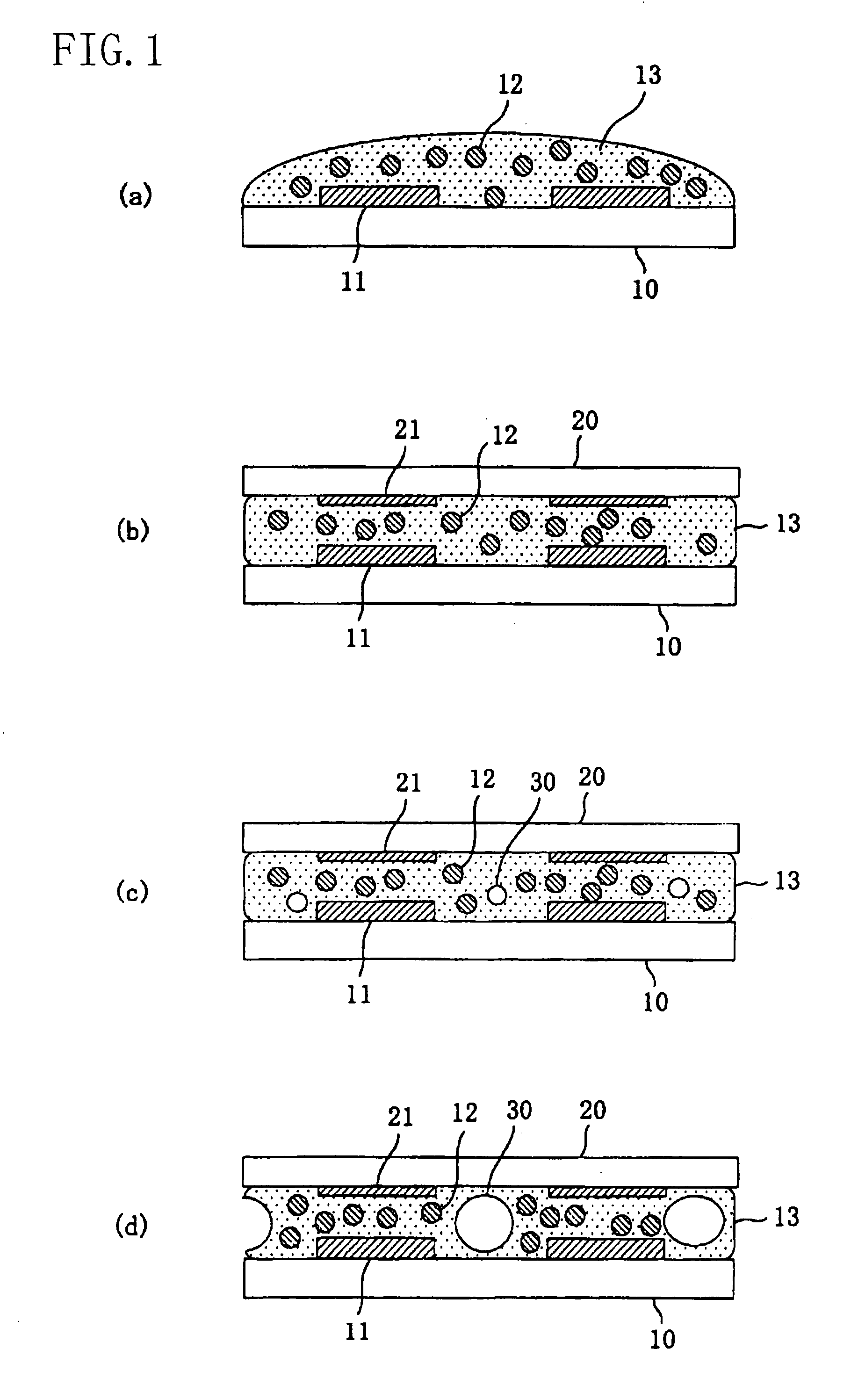
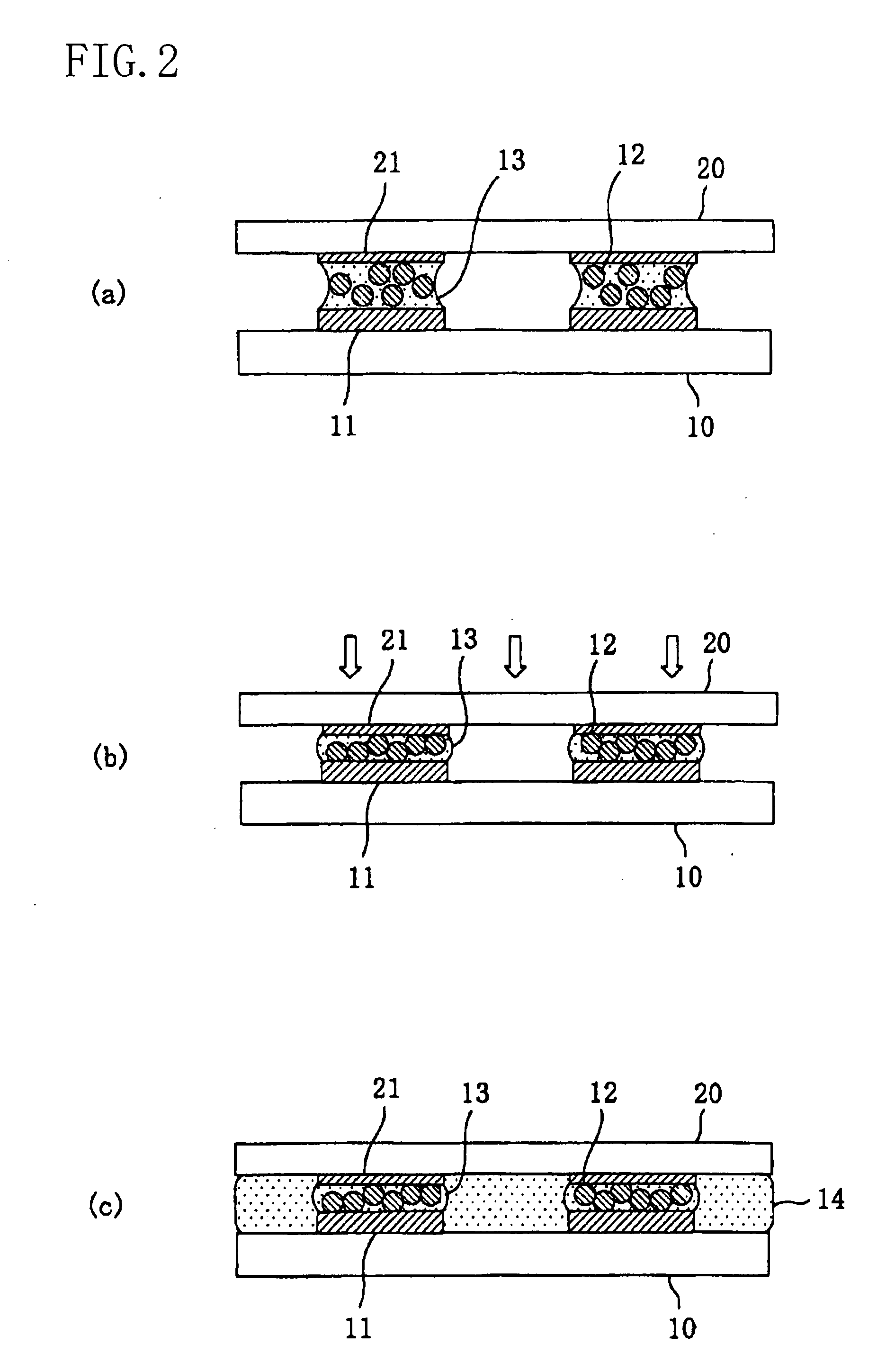
[0067]FIGS. 1(a) to 1(d) and FIGS. 2(a) to 2(c) are step-by-step cross-sectional views showing the basic steps of a flip chip mounting method in an embodiment of the present invention.

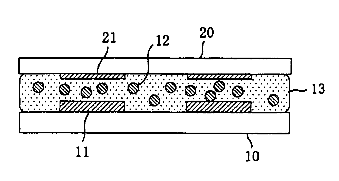
[0068]First, as shown in FIG. 1(a), a resin (e.g., an epoxy resin or the like) 13 containing conductive particles (e.g., Cu or the like) 12 and a gas bubble generating agent (e.g., isopropyl alcohol or the like) is supplied onto a circuit board 10 having a plurality of connecting terminals 11. Then, as shown in FIG. 1(b), a semiconductor chip 20 having a plurality of electrode terminals 21 is disposed on the surface of the resin 13 to face the circuit board 10. At this time, the electr...


PUM


Abstract

A flip chip mounting method which is applicable to the flip chip mounting of a next-generation LSI and high in productivity and reliability as well as a method for connecting substrates are provided. A circuit board 10 having a plurality of connecting terminals 11 and a semiconductor chip 20 having a plurality of electrode terminals 21 are disposed in mutually facing relation and a resin 13 containing conductive particles 12 and a gas bubble generating agent is supplied into the space therebetween. In this state, the resin 13 is heated to generate gas bubbles 30 from the gas bubble generating agent contained in the resin 13. The resin 13 is pushed toward the outside of the generated gas bubbles 30 by the growth thereof. The resin 13 pushed to the outside is self-assembled in the form of columns between the respective terminals of the circuit board 10 and the semiconductor chip 20. In this state, by pressing the semiconductor chip 20 against the circuit board 10, the conductive particles 12 contained in the resin 13 self-assembled between the facing terminals are brought into contact with each other to provide electrical connection between the terminals.

Description

RELATED APPLICATIONS[0001]This application is the U.S. National Phase under 35 U.S.C. § 371 of International Application No. PCT / JP 2006 / 305274, filed on Mar. 16, 2006, which in turn claims the benefit of Japanese Application No. 2005-094233, filed on Mar. 29, 2005, the disclosures of which Applications are incorporated by reference herein.TECHNICAL FIELD[0002]The present invention relates to a flip chip mounting method for mounting a semiconductor chip on a circuit board and to a method for connecting substrates each formed with a plurality of electrodes.BACKGROUND ART[0003]In recent years, as semiconductor integrated circuits (LSIs) used in electronic equipment have become higher in density and degree of integration, the electrode terminals of LSI chips have rapidly become higher in pin count and narrower in pitch. To mount such an LSI chip on a circuit board, flip chip mounting has been used widely for a reduction in wiring delay. In the flip chip mounting, it is typical to form ...

Claims


Application Information

Patent Timeline
Patent Type & Authority Applications(United States)
IPC IPC(8): H01L21/02H01L23/498
CPCH01L21/563H01L24/16H01L24/27H01L24/29H01L24/73H01L24/83H01L25/0657H01L25/50H01L2224/13099H01L2224/1319H01L2224/16148H01L2224/16225H01L2224/16227H01L2224/165H01L2224/2929H01L2224/29291H01L2224/293H01L2224/29339H01L2224/29347H01L2224/73204H01L2224/75H01L2224/83047H01L2224/83091H01L2224/83097H01L2224/83192H01L2224/83204H01L2224/83862H01L2224/8388H01L2224/83886H01L2224/83887H01L2225/06513H01L2924/01002H01L2924/01004H01L2924/01005H01L2924/01009H01L2924/01013H01L2924/01015H01L2924/01027H01L2924/01029H01L2924/01033H01L2924/01047H01L2924/0105H01L2924/01078H01L2924/01082H01L2924/14H01L2924/30105H01L2924/381H05K3/323H05K2201/10674H05K2203/087H01L2224/2919H01L2924/01006H01L2924/01019H01L2924/01067H01L2924/014H01L2924/0665H01L2224/29101H01L2924/0132H01L2924/1579H01L2224/29111H01L2224/13339H01L2224/13347H01L2224/1329Y10T156/1744H01L2924/00011H01L2924/066H01L2924/00015H01L2924/00H01L2924/00014
Inventor KARASHIMA, SEIJIKITAE, TAKASHINAKATANI, SIICHI
Owner PANASONIC CORP
Why Eureka
Try Eureka