Multiple gate field effect transistor structure and method for fabricating same

Inactive Publication Date: 2009-05-14
S O I TEC SILICON ON INSULATOR THECHNOLOGIES
View PDF9 Cites 24 Cited by
  • Summary
  • Abstract
  • Description
  • Claims
  • Application Information

AI Technical Summary

Benefits of technology

[0011]It has been shown as advantageous if the upper silicon oxide layer is formed with a thickness of 2 to 20 nm, preferably with a thickness of 5 to 15 nm, and more preferably with a thickness of 3 to 12 nm. Because the total height of the fin is given by the sum of the thickness of the semiconductor layer used to make the fin plus the thickness of the silicon oxide layer undercut below the fin, the smaller the upper oxide layer the lower is the total fin height variation. On the other hand, a certain thickness of the upper oxide layer is necessary to allow a formation of rounded corners at the bottom of the fin during etching and cleaning steps of the fin fabrication process. The above thickness values of 2 to 20 nm are a compromise between the above mentioned requirements, wherein with the thickness values of 5 to 15 nm a low undercut can be combined with a good roundness of the corners, and thickness values of 3 to 12 nm

Problems solved by technology

A silicon nitride layer directly under the semiconductor layer from which the fin is formed, results in a minimum vertical recess and fin undercut.
However, if silicon nitride is used as insulator material directly under

Method used


Image

  • Multiple gate field effect transistor structure and method for fabricating same
  • Multiple gate field effect transistor structure and method for fabricating same
  • Multiple gate field effect transistor structure and method for fabricating same

Examples


first embodiment

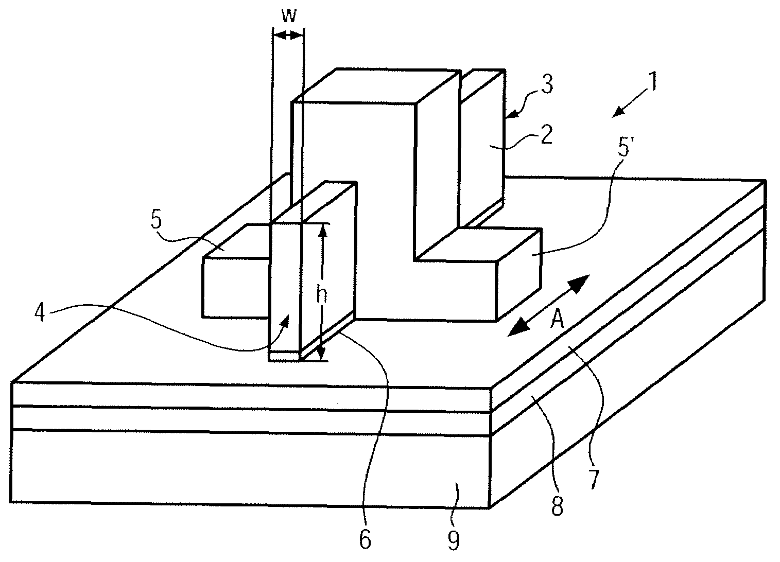
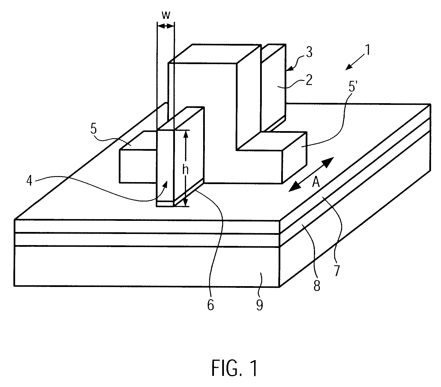
[0036]FIG. 3 shows schematically a geometry of a fin 2 according to the present invention. The fin 2 is formed on the surface of a silicon nitride layer 7 with a thickness of 10 to 30 nm, the silicon nitride layer 7 being formed on top of an oxide layer 8 with a thickness of 70 to 80 nm.

[0037]During the formation of the fin 2, the underlying silicon nitride layer 7 acts as an etch stop and reduces, therefore, greatly the vertical recess V and the lateral recess and undercut of the fin 2. According to a particular example, it has been shown that the vertical recess V went to a 2 nm to 4 nm range from about 15 nm and that the horizontal recess was completely reversed. As a consequence of reversing of the profile of the lateral recess or undercut of the fin 2, the bottom corner profile of the fin 2 changes from rounded to tapered which might not be a desirable effect.

second embodiment

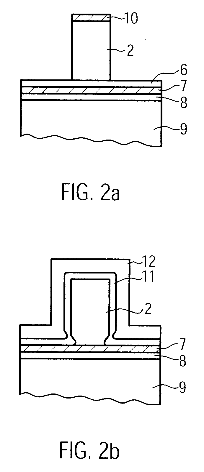
[0038]FIG. 4 shows schematically a geometry of a fin 2′ according to the present invention. The fin 2′ is formed on a layer stack consisting of a lower silicon oxide layer 8, a silicon nitride layer 7 and an upper silicon oxide layer 6 formed on top of the layer stack directly under the fin 2′. That means, in comparison to the example shown in FIG. 3, the top nitride layer 7 is replaced by the 10 nm to 15 nm range top oxide layer 6. By means of the upper silicon oxide layer 6, the advantage of rounded corners when etching and subsequently cleaning the fin 2′ during the fabrication process can be conserved. As shown in FIG. 4, there is not only a vertical recess V but also a horizontal recess H in the region under the fin 2′, leading to rounded corner formation at the bottom of the fin 2′. Moreover, the used layer structure keeps the benefit of perfectly controlling the fin 2′ vertical recess V by using the silicon nitride layer 7 as a hard etch stop when the silicon oxide layer 6, u...

third embodiment

[0039]FIG. 5 shows schematically a geometry of a fin 2″ according to the present invention. The fin 2″ is an improved variant of the fin 2′ of FIG. 4. The fin 2″ was well controlled over-etched in order to increase the undercut below the fin 2″. The larger horizontal recess H helps to round the bottom corners of the fins, which helps to improve the propagation of the gate electric field of the resulting FinFET 1 for a better back-gate effect.

[0040]FIG. 6 shows the same geometry of the fin 2″ according to the third embodiment of the present invention shown in FIG. 5, whereas the thickness of the upper silicon oxide layer 6 is reduced by half. This reduces by about the same value the horizontal recess H and helps to achieve a better compromise between recess profile and bottom corner rounding of the resulting fin 2′″.

H˜½TSi02Fin

The total height h variation of the fin 2′, 2″, 2′″ including the vertical recess V on each side of the fin 2′, 2″, 2′″ is given by the sum of the thickness T...


PUM


Abstract

The present invention relates to a Multiple Gate Field Effect Transistor structure and a method for fabricating same. The Multiple Gate Field Effect Transistor structure includes a fin structure made from at least one active semiconductor layer of a silicon on insulator (SOI) structure on a buried insulator of the structure. The Multiple Gate Field Effect Transistor structure also includes an insulator of at least one high-k layer of a material having a dielectric constant that is higher than silicon oxide. This has the advantage that the high-k layer acts as a better etch stop than silicon oxide during formation and cleaning of the fin resulting in a lower recess and undercut effect on the socket of the fin. This leads to a higher stability of the formed fin and enables a smooth finishing of the fin by etching and cleaning steps.

Description

BACKGROUND[0001]The present invention relates to a Multiple Gate Field Effect Transistor structure having a fin-like structure for forming therein a transistor channel of the multiple gate field effect transistor structure. The fin-like structure is formed from at least one active semiconductor layer of a Silicon On Insulator (SOI) structure on a buried insulator of the SOI structure. The present invention also relates to a method for fabricating such structures. This method comprises providing a SOI substrate comprising at least one active semiconductor layer, a buried insulator and a carrier substrate, and forming from the semiconductor layer a fin structure on the insulator, wherein the fin structure forms a region for a transistor channel of the Multiple Gate Field Effect Transistor structure.[0002]Scaling of device dimensions is a primary factor driving improvements in integrated circuits manufacturing. Due to limitations in scaling gate oxide thickness and source / drain junctio...

Claims


Application Information

Patent Timeline
IPC IPC(8): H01L29/00H01L21/20
CPCH01L29/42392H01L29/66795H01L29/78696H01L29/7853H01L29/78603H01L29/785H01L29/772
Inventor PATRUNO, PAUL
Owner S O I TEC SILICON ON INSULATOR THECHNOLOGIES
Why Eureka
Try Eureka