
Nanowire-based sensor configurations

a sensor configuration and nanowire technology, applied in the field of nanowire-based sensor configurations, can solve the problems of insufficient adaptability, high cost, and insufficient spectrophotometric detection, and achieve the effects of increasing hydrodynamic drag, enhancing sensitivity and/or range of analysis, and increasing the ra

Active Publication Date: 2009-05-14
NANOSYS INC
View PDF54 Cites 50 Cited by
  • Summary
  • Abstract
  • Description
  • Claims
  • Application Information

AI Technical Summary

Benefits of technology

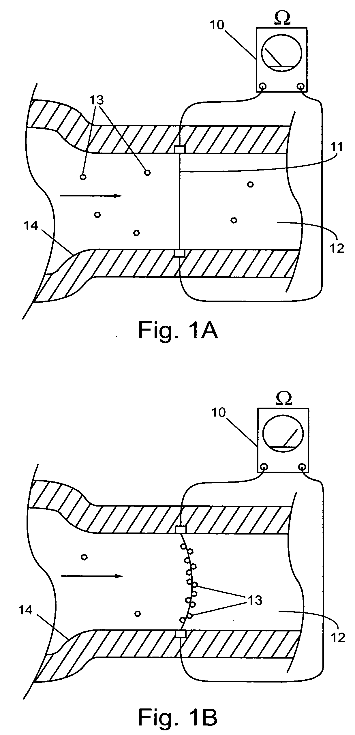
[0014]In one aspect of the invention, the nanowire can be mounted to a piezojunction. The nanowire can be a semiconductor wire, or carbon based nanotube, with adequate tensile strength and / or rigidity to transfer physical stresses to the piezojunction. In the piezojunction embodiment, the nanowire can have, e.g., molecular binding sites for the analyte. The chamber can be a channel with a flowing fluid, so that, e.g., binding of the analyte to the binding sites increases the hydrodynamic drag of the fluid on the nanowire, resulting in stress and a detectable change in the electrical parameter at the piezojunction (typically detectable as a changed electrical parameter in a circuit through the junction). The chamber can be, e.g., a channel with a constriction where the nanowire is mounted to accelerate fluid flow at the site of the nanowire sensor. The constriction can be, e.g., caused by a buildup of analyte molecules at binding sites on the channel surface.
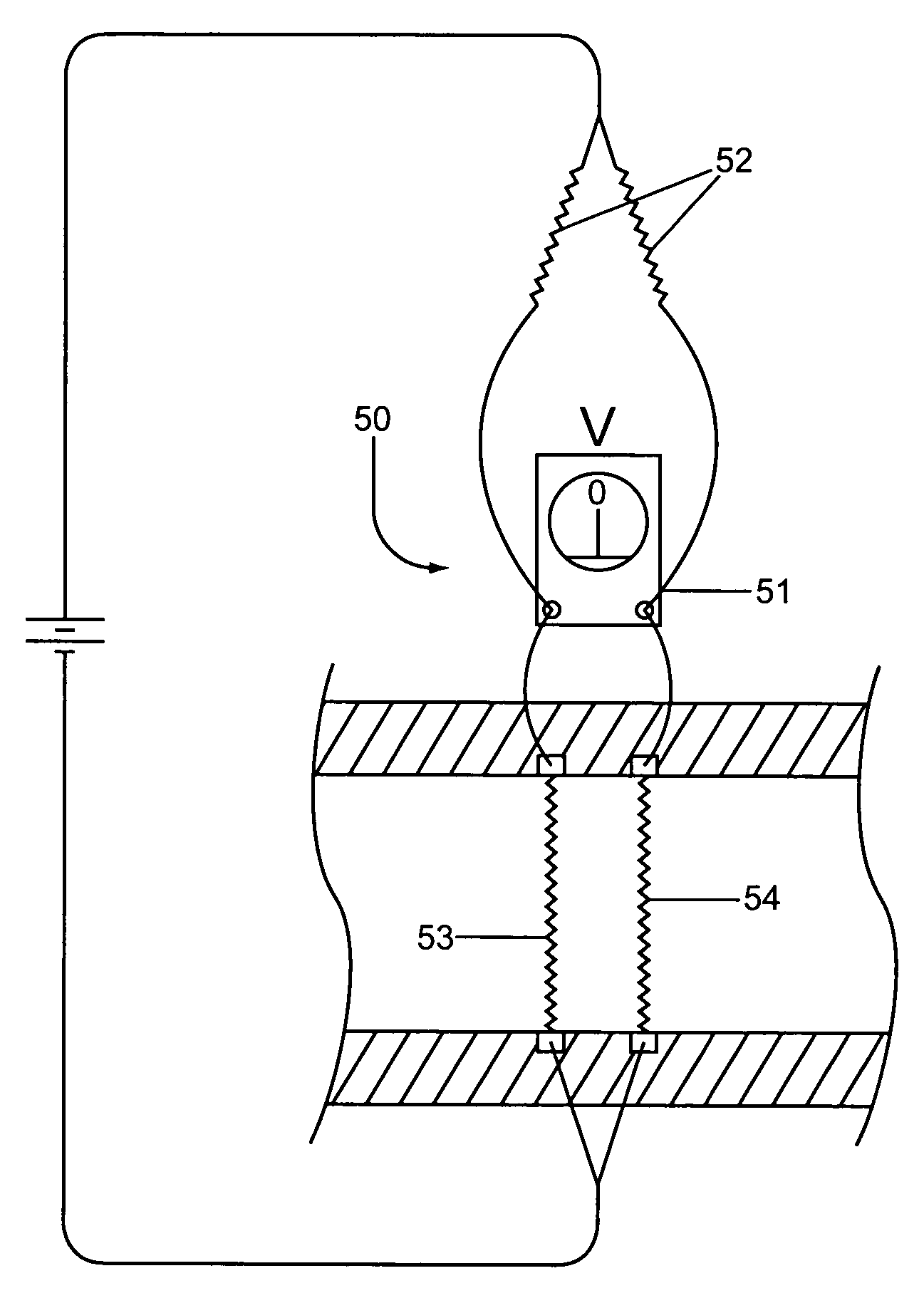
[0024]In other embodiments, such as in methods involving DNA hybridization or field effects of analytes, sensitivity, specificity, and / or quantitative range can be enhanced, e.g., by washing the nanowire with a low ionic strength solution before detecting the change in the electrical parameter. The sensitivity and accuracy of the methods can be enhanced, e.g., by comparing the electrical parameter change associated with a test nanowire to an electrical parameter associated with a control nanowire. In methods for detection of analytes eluting from an electrophoretic separation, e.g., detection of changed electrical parameters can be enhanced by shutting off electrophoretic current before detecting a change.

Problems solved by technology

Detectors used in analytical methods and screening protocols are often nonspecific, require complex chromogenic interactions, or are not well adapted to microscale systems.
Such spectrophotometric detection is generally nonspecific, can be expensive, and often yields relatively high signal to noise ratios, particularly when detecting very small concentrations of analyte.
These affinity based systems can provide specific detection of molecules, but in addition to the above-mentioned difficulties, can also require the use of hazardous materials and complex plumbing for assay automation.
These detectors are typically not useful in detection of biological molecules for lack of specificity and sensitivity.
In addition, the high impedance required for many of these detectors to sense changes in microenvironments can provide a noisy signal with poor sensitivity.
Beam style piezoelectric detection devices require a complex multilayered etching and coating technology, produce microscale (but not nanoscale) sensor elements, and can have a disadvantageous ratio of binding surface to sensor mass.
While such chemically sensitive field effect transistors (or ChemFETs) have shown some functionality, the requirement of very large concentrations of charged analyte to achieve a detectable gating of the transistor has resulted in their not being particularly useful for most applications.

Method used


Image

  • Nanowire-based sensor configurations
  • Nanowire-based sensor configurations
  • Nanowire-based sensor configurations

Examples


Embodiment Construction

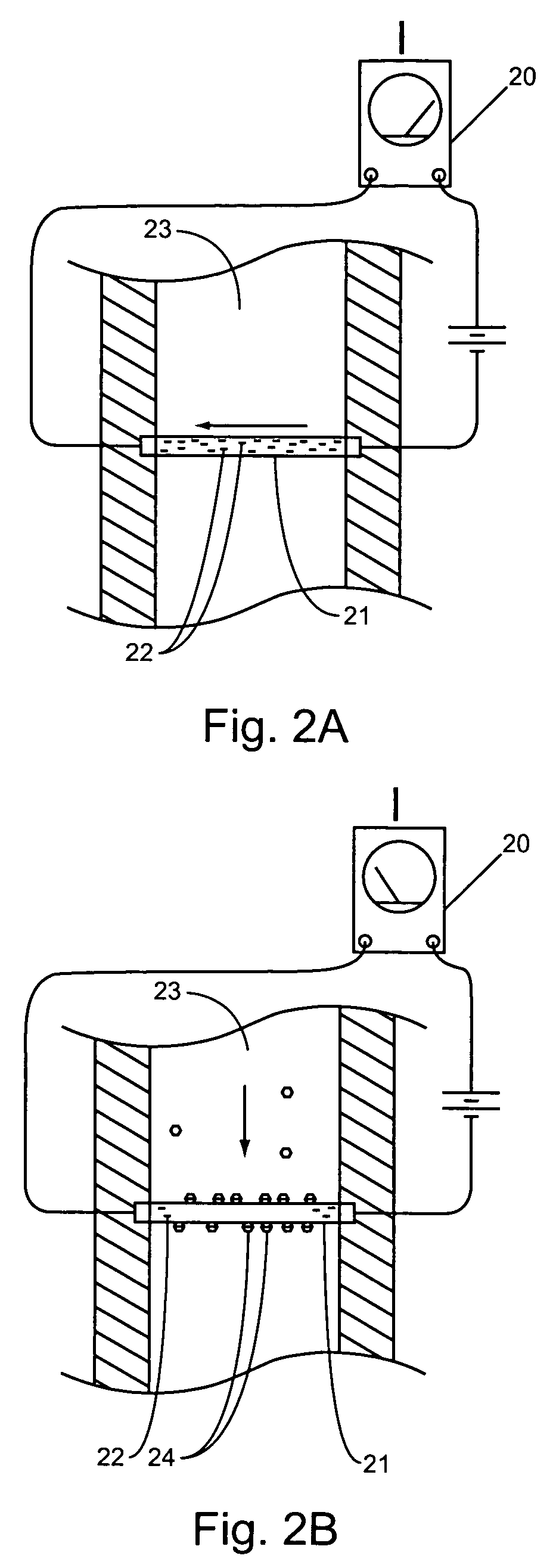
[0038]Nanowire-based sensor configurations of the invention provide, e.g., sensors and methods to detect analytes in process, analysis, and / or microfluidic systems. The sensors can be, e.g., nanowires mounted in chambers and in electrical contact with electrical parameter detectors for detection of changes in the nanowire electrical properties on interaction with an analyte. The methods for sensing analytes can include, e.g., contacting a nanowire mounted in a chamber of a microfluidic system with an analyte, and detecting a change in an electrical parameter associated with the nanowire to sense the analyte. The sensors and methods of the invention can be used, e.g., to detect analytes of interest in chromatographic separations and / or sample cells of microarrays.

Nanowire-Based Sensors

[0039]The sensors of the invention include, for example, nanowires mounted in chambers of devices wherein the presence of an analyte of interest induces a detectable change in an electrical parameter as...


PUM

PropertyMeasurementUnit
Electrical resistanceaaaaaaaaaa
Electric fieldaaaaaaaaaa
Ionic strengthaaaaaaaaaa

Abstract

This invention provides nanowire based molecular sensors and methods for detecting analytes in a microfluidic system. Methods for sensing analytes include detecting changed electrical parameters associated with contact of a nanowire with the analyte in a microfluidic system. Sensors of the invention include nanowires mounted in microchambers of a microfluidic system in electrical contact with the detector, whereby electrical parameter changes induced in the nanowire by the analyte can be monitored by the detector.

Description

CROSS-REFERENCE TO RELATED APPLICATION[0001]This application is a divisional of U.S. patent application Ser. No. 10 / 853,006, filed May 25, 2004, which claims the benefit of U.S. Provisional Patent Application No. 60 / 475,831 filed Jun. 3, 2003, the full disclosures of which are hereby incorporated herein by reference in their entirety for all purposes.STATEMENT AS TO RIGHTS TO INVENTIONS MADE UNDER FEDERALLY SPONSORED RESEARCH AND DEVELOPMENT[0002]A portion of this invention was made under SBIR Grants from the National Institutes of Health, Grant Numbers 1 R43A152533-01 and 1 R43CA101567-01, and the government may have certain rights in the inventions.FIELD OF THE INVENTION[0003]The present invention is in the field of sensors for detection of analytes. The sensors of the invention can detect molecular species, e.g., in a chromatographic elution or in an array. Sensors of the invention are suitable for incorporation into analytical systems, including capillary based and microscale fl...

Claims


Application Information

Patent Timeline
IPC IPC(8): G01N33/551G01N33/543G01N33/53
CPCB82Y15/00G01N33/54313G01N27/4146G01N27/127
Inventor HAMILTON, JAMES M.DUBROW, ROBERT S.CHOW, CALVIN Y.H.
Owner NANOSYS INC
Learn More