Method of fabricating flash memory

a technology of flash memory and stacked structures, applied in the direction of basic electric elements, electrical equipment, semiconductor devices, etc., can solve the problems of reducing adhesion, reducing the adhesion, and oxidizing the sidewall abnormally, so as to improve the silicon/tungsten distribution ratio and improve the word line resistan

Inactive Publication Date: 2009-05-21
POWERCHIP SEMICON CORP
View PDF0 Cites 3 Cited by
  • Summary
  • Abstract
  • Description
  • Claims
  • Application Information

AI Technical Summary

Benefits of technology

[0011]It is an advantage of the claimed invention that a silicon cap layer is formed on the sidewall surface of the silicide layer prior to performing the thermal process for oxidizing the silicon cap layer into an oxide layer, such that the structure of the silicide layer can be effectively protected to prevent the silicide layer from damaging or

Problems solved by technology

However, as shown in FIG. 2, an unsuitable thermal process will cause side effect to erode portions of the silicide layer 22 and cause abnormal oxidization of the sidewall of the stacked structures 28 such that the oxide layer 26 with an abnormal large thickness is formed on the sidewall of the silicide layer 22 for example.
Under this situation, voids are easily formed between adjacent stacked structures 28, resulting in that the following formed materials cannot fully fill in the area between the stacked structures 28.
In addition, the thermal process also reduces the adhesion of the silicide layer 22, thus the word line easily peels off.
As a result, although the prior arts provide the thermal process for reducing the sheet resistance of the word line, an unsuit

Method used


Image

  • Method of fabricating flash memory
  • Method of fabricating flash memory
  • Method of fabricating flash memory

Examples


first embodiment

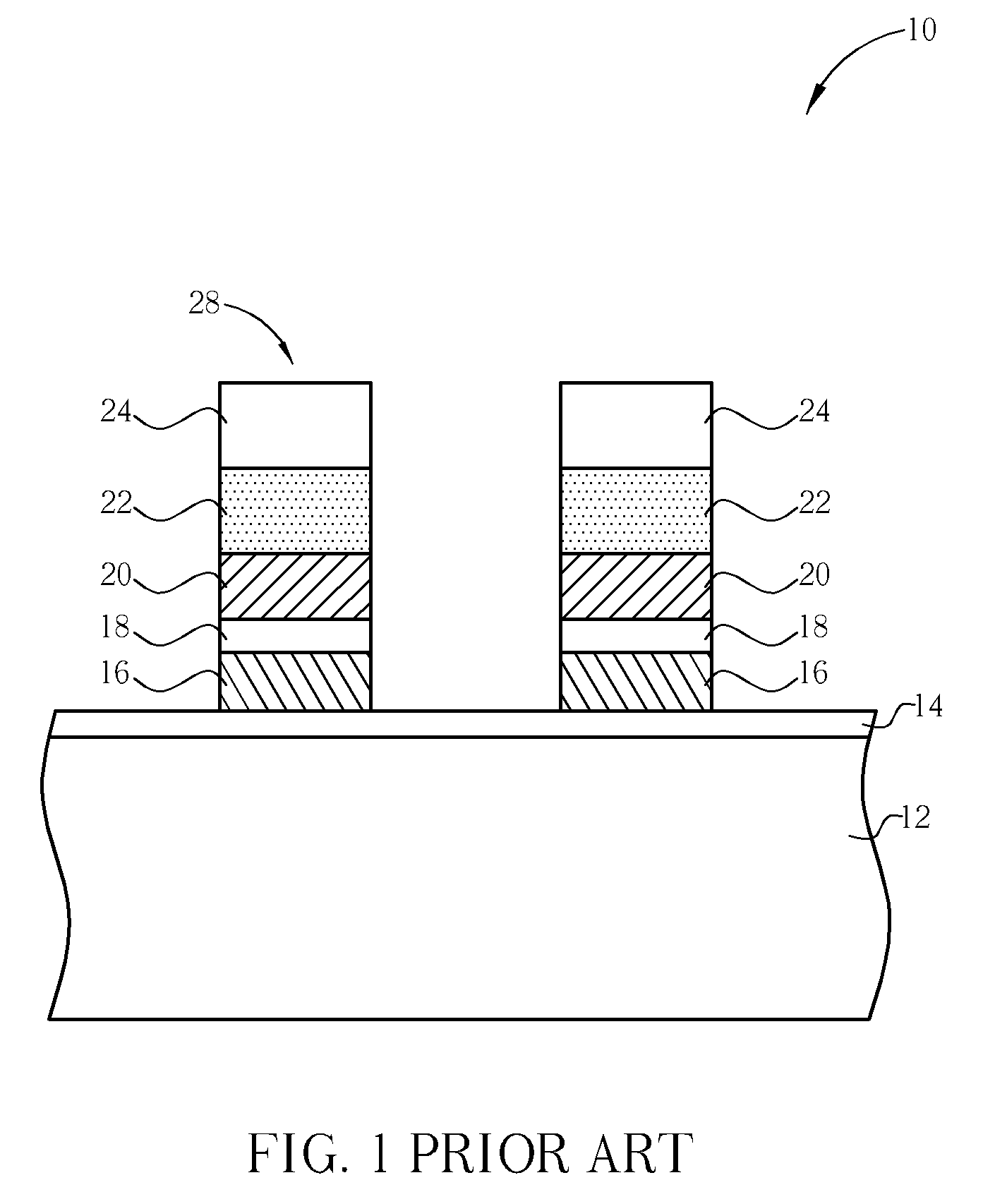
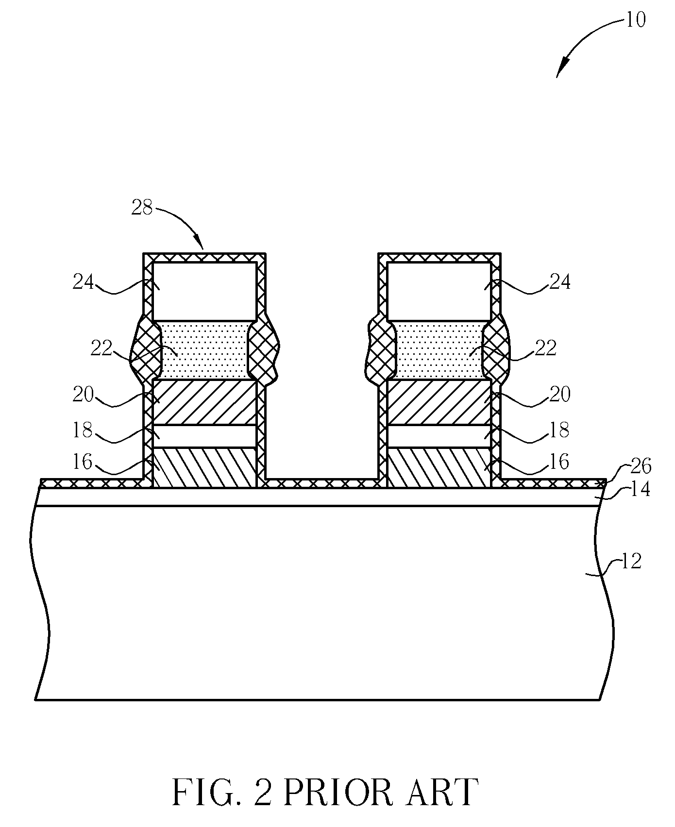
[0016]Referring to FIGS. 3-8, FIGS. 3-8 are process schematic diagrams of the fabrication method of a flash memory 50 according to the present invention. The present flash memory 50 is a stack-gate flash memory. First, as shown in FIG. 3, a semiconductor substrate 52 is provided, which may be a silicon substrate. An oxidization process is carried out to form an oxide layer on the surface of the semiconductor substrate 52, wherein the oxide layer serves as a floating gate insulating layer 54. Then, a floating gate material layer 56, a dielectric layer 58, a control gate material layer 60, a silicide layer 62, and a hard mask layer 64 are successively formed on the surface of the semiconductor substrate 52. The floating gate material layer 56 and the control gate material layer 60 preferably comprise polysilicon material layer respectively, and the silicide layer 62 may comprise tungsten silicide material. The hard mask layer 64 may comprise silicon nitride material, while the dielect...

second embodiment

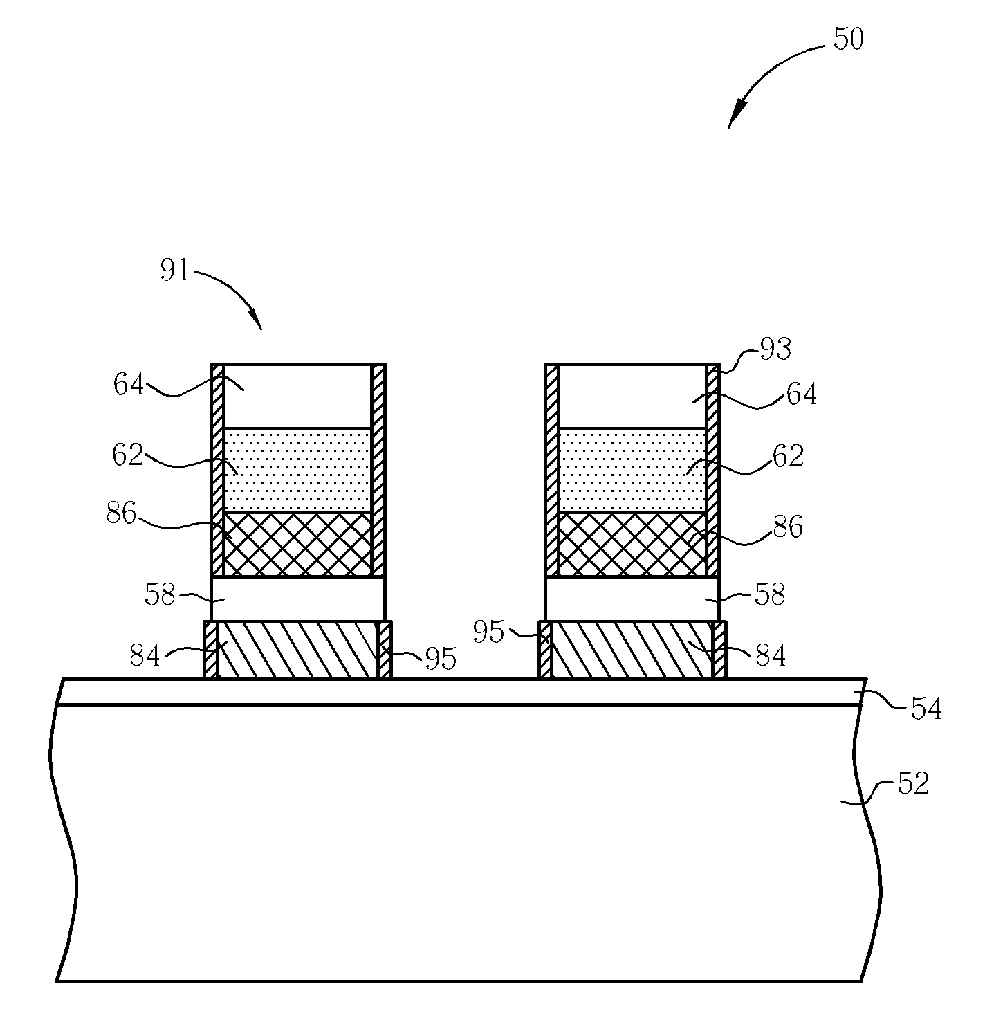
[0021]FIGS. 9-12 are process schematic diagrams of the fabrication method of a flash memory according to the present invention. Some devices in FIGS. 9-12 are indicated by the same numerals as those used in FIGS. 3-8 for simplifying the description, and FIG. 9 illustrates a subsequent process and structure profile of the flash memory 50 of FIG. 3. A floating gate material layer 56, a dielectric layer 58, a control gate material layer 60, a silicide layer 62, and a hard mask layer 64 are successively formed on the semiconductor substrate 52, wherein the dielectric layer 58 may be an ONO dielectric layer or a NONON dielectric layer. Then, as shown in FIG. 9, an photolithography process is performed to pattern the hard mask layer 64 so that the hard mask layer 64 has at least a control gate pattern 87. Sequentially, the patterned hard mask layer 64 is taken as a mask for performing an etching process to the silicide layer 62 and the control gate material layer 60 until the top surface ...


PUM


Abstract

A method of fabricating a flash memory includes successively forming a floating gate insulating layer, a floating gate material layer, a dielectric layer, a control gate material layer, a silicide layer, and a hard mask layer on a semiconductor substrate, patterning the hard mask layer, removing portions of the silicide layer, the control gate material layer, the dielectric layer, and the floating gate material layer not covered by the hard mask layer to form a stacked structure, forming a silicon cap layer covering the surface of the stacked structure, and performing a thermal process.

Description

BACKGROUND OF THE INVENTION[0001]1. Field of the Invention[0002]The present invention relates to a method of fabricating a flash memory, and more particularly, to a method of fabricating a flash memory by utilizing a silicon cap layer to improve the structure and performance of the flash memory.[0003]2. Description of the Prior Art[0004]Because a nonvolatile memory cell is rewritable and has qualities as fast transfer and low power consumption, it has been widely applied to products of various fields and become a critical device of many information, communication, and consuming electronic products. However, in order to provide light electronic products with high quality, it has become important for the current information industry and memory manufacturers to increase the device integration and quality of the nonvolatile memory cells.[0005]Please refer to FIGS. 1-2. FIGS. 1-2 are schematic diagrams of a fabrication method of a stack-gate flash memory 10 according to the prior art. As...

Claims


Application Information

Patent Timeline
IPC IPC(8): H01L21/336
CPCH01L27/11521H01L29/7881H01L29/66825H10B41/30
Inventor LO, CHAO-YUANYOUNG, REXWANG, PIN-YAO
Owner POWERCHIP SEMICON CORP
Why Eureka
Try Eureka