Organic Photovoltaic Device With Improved Power Conversion Efficiency And Method Of Manufacturing Same

Inactive Publication Date: 2009-05-28
KOREA INST OF SCI & TECH
View PDF3 Cites 5 Cited by
  • Summary
  • Abstract
  • Description
  • Claims
  • Application Information

AI Technical Summary

Benefits of technology

[0009]The primary object of the present invention is to provide an organic photovoltaic device capable of maintaining high power conversion efficiency through a lowering of series resistance even though it is fabricated as a large area device.
[0010]In accordance with one embodiment of the present invention for achieving the above object, there is provided a method of fabricating an organic photovoltaic device wit

Problems solved by technology

Unfortunately, such research is currently at a standstill.
When an organic thin layer photovoltaic cell using fullerene having high electron mobility was introduced for the first time in 1993, such a device did not come into the spotlight due to its extremely low power conversion efficiency (N. S. Sariciftci, et al., Appl. Phys. Left. 62: 585, 1993; J. J. M. Halls, et al., Appl. Phys. Lett. 68: 3120, 1996).
Based on t

Method used


Image

  • Organic Photovoltaic Device With Improved Power Conversion Efficiency And Method Of Manufacturing Same
  • Organic Photovoltaic Device With Improved Power Conversion Efficiency And Method Of Manufacturing Same
  • Organic Photovoltaic Device With Improved Power Conversion Efficiency And Method Of Manufacturing Same

Examples


Example

Example 1

Fabrication of an Organic Photovoltaic Device by Active Area Partitioning

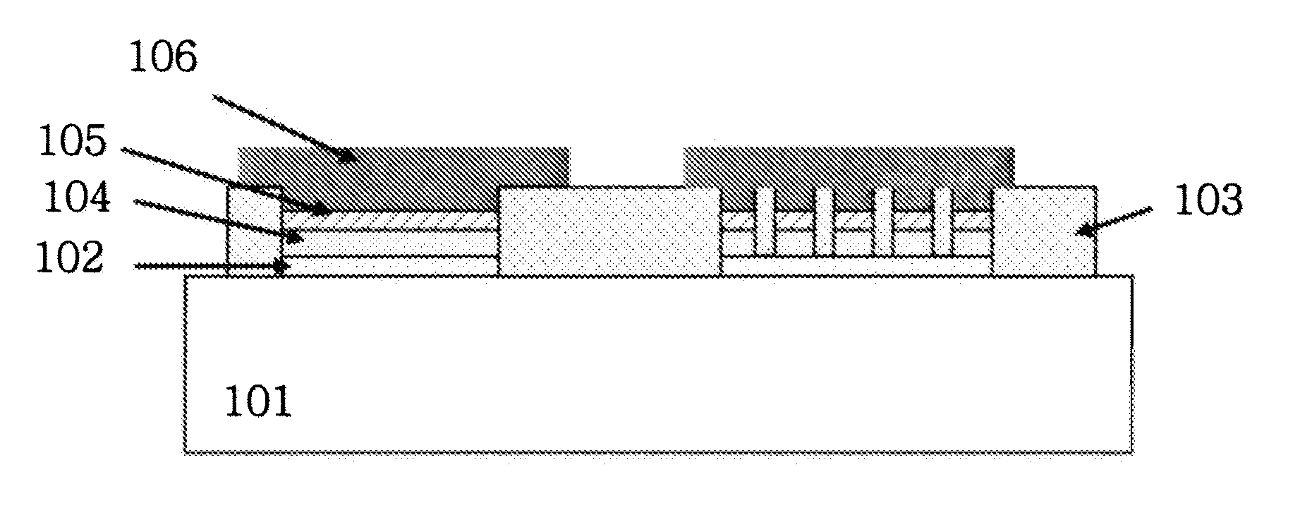
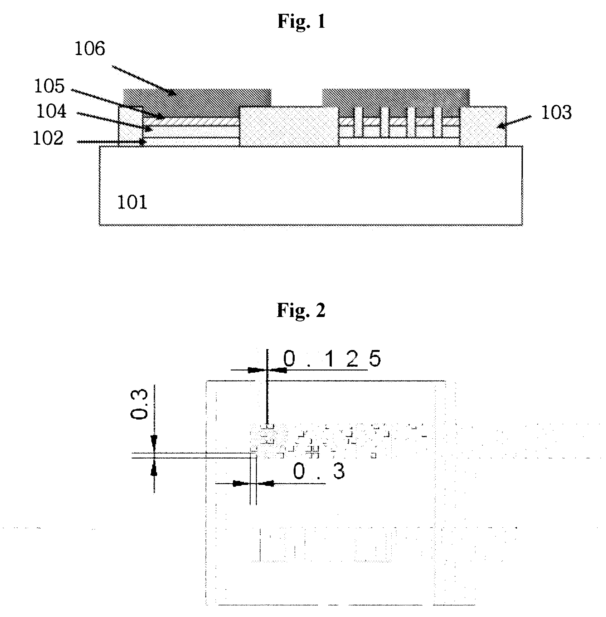
[0057]As illustrated in FIG. 2, the following process was carried out to fabricate a single device wherein both the small area of an organic photovoltaic device formed by active area partitioning with insulating partitioning walls introduced into the device according to the method of the present invention and the large area organic photovoltaic device formed according to the prior art method are formed thereon. At this time, the organic photovoltaic device was prepared by spin coating a P3HT / PCBM blend, which is the representative organic blend useful for forming a bicontinuous interpenetrating network structure, on a transparent electrode, and depositing aluminum as an electrical charge extraction electrode thereon. When a single large area cell with no partitioning wall and a plurality of small area subcells including partitioning walls are formed in a single device like this, it is possible to reduc...

Example

Example 2

Characteristic Analysis of an Organic Photovoltaic Device

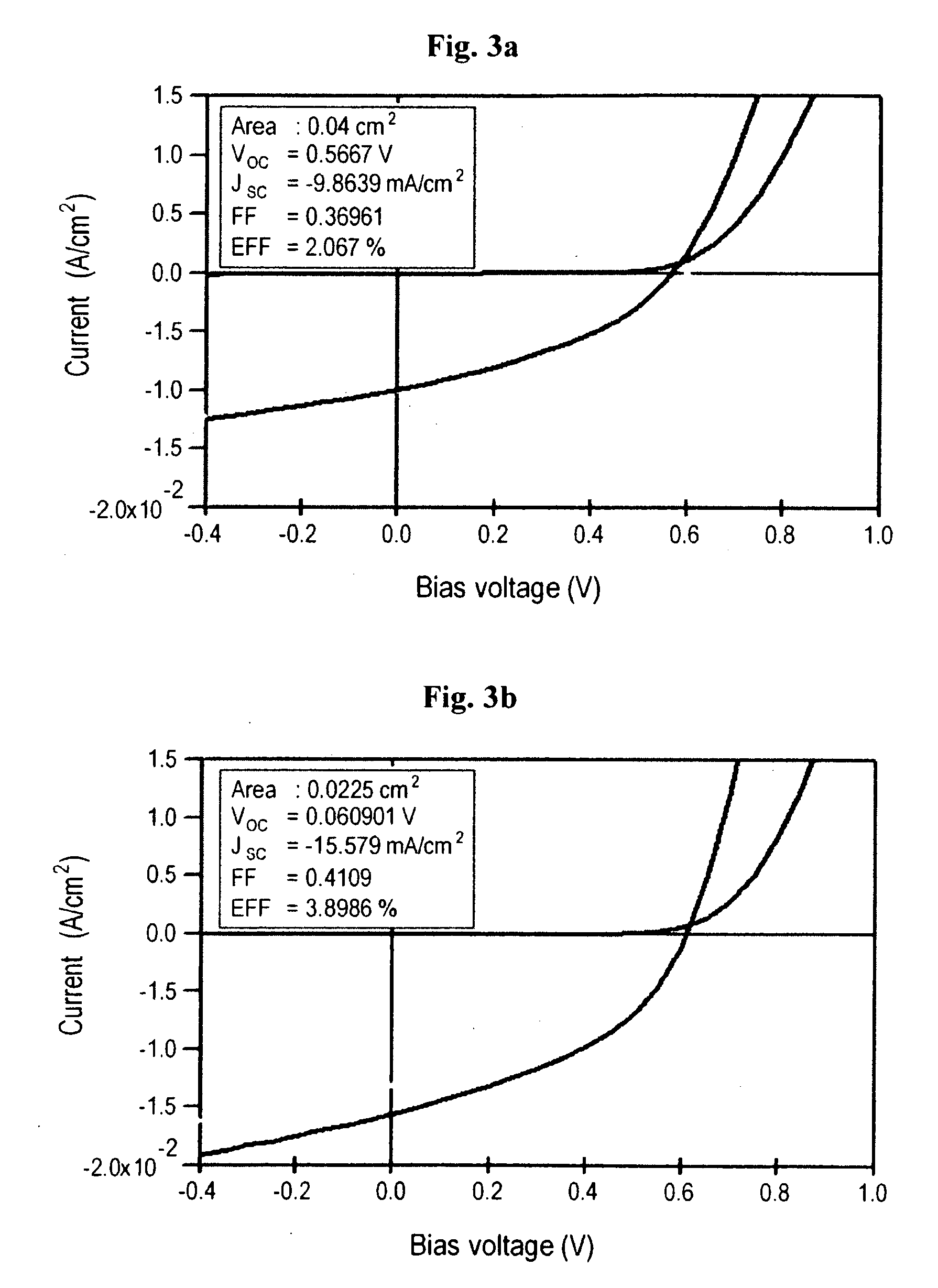
[0063]A current-voltage (I-V) characteristic of the organic photovoltaic device fabricated in Example 1 was measured by using a Keithley 2400 source-measure unit. The results are shown in FIGS. 3a and 3b. At this time, a Xe lamp (300 W) was used as a light source. Further, the strength of light was regulated by using an air mass filter (AM 1.5, Oriel) under the illumination condition of imitating an irradiation wavelength of sunlight, in combination with the use of a neutral density filter if necessary. The strength of light irradiation was measured by using a calibrated broadband optical power meter (Spectra Physics model 404).

[0064]As shown in FIG. 3a, the open circuit voltage of the organic photovoltaic device fabricated according to the prior art method was 0.56697 V, the short circuit current density thereof was 9.8639 mA / cm2, the fill factor thereof was 0.36961, and the power conversion efficiency thereof was 2....

Example

Example 3

Change in Power Conversion Efficiency Depending on Conductivity of an Electrode Protection Layer

[0065]In order to examine the effect of a correlation between conductivity of an electrode protection layer and active area partitioning on power conversion efficiency in the organic photovoltaic device according to the present invention, the electrode protection layer was formed by using Baytron A1 4083 (Bayer) having a conductivity of 10−3 S / cm instead of using the Baytron P layer having a conductivity of 1 S / cm. Except for using Baytron A1 4083 as an electrode protection layer, the organic photovoltaic device through active area partitioning according to the method as described in Example 1 and the organic photovoltaic device according to the prior art method were also fabricated in a single cell device. Their current-voltage characteristics were analyzed according to the same method as described in Example 2.

[0066]As a result, as can be seen in FIG. 4a, the organic photovolta...


PUM

PropertyMeasurementUnit
Transparencyaaaaaaaaaa
Power conversion efficiencyaaaaaaaaaa
Electron affinityaaaaaaaaaa

Abstract

The present invention relates to a method of fabricating an organic photovoltaic device with improved power conversion efficiency by reducing lateral contribution of series resistance between subcells through active area partitioning by introducing a patterned structure of insulating partitioning walls inside the device. According to the method of the present invention, since the lateral contribution of series resistance between the partitioned subcells is minimized and each subcell works independently, there is no interference phenomenon against the current output of each subcells. As such, the function of a charge extraction layer with high conductivity can be maximized. Thus, the method of the present invention can be effectively used in the fabrication and development of a next-generation large area organic thin layer photovoltaic cell device.

Description

[0001]The present application claims priority from Korean Patent Application No. 10-2007-120363 filed Nov. 23, 2007, the entire contents of which are incorporated herein by reference.FIELD OF THE INVENTION[0002]The present invention relates to a method of manufacturing an organic photovoltaic device with improved power conversion efficiency by reducing lateral contribution of series resistance which obtained by partitioning off an active layer through the introduction of a patterned insulating walls inside the device. The present invention further relates to an organic photovoltaic device manufactured using the above method.BACKGROUND OF THE INVENTION[0003]Extensive research for improving power conversion efficiency has been actively performed ever since an organic thin layer solar (photovoltaic) cell having power conversion efficiency of about 1% was developed by Tang in 1986 (C. W. Tang, Appl. Phys. Lett. 48: 183, 1986). Unfortunately, such research is currently at a standstill. A...

Claims


Application Information

Patent Timeline
IPC IPC(8): H01L31/00B05D5/12C23C14/34G03F7/20B29C35/08H01L21/02
CPCH01L27/301H01L51/0036Y02E10/549H01L51/4253H01L51/445H01L51/0037H10K39/10H10K85/1135H10K85/113H10K30/83H10K30/30H10K30/00
Inventor YU, JAE-WOONGCHIN, BYUNG DOOKIM, JAI KYEONGKANG, NAM SOO
Owner KOREA INST OF SCI & TECH
Why Eureka
Try Eureka