

Light emitting device and method of producing light emitting device
a technology of light emitting device and light emitting device, which is applied in the direction of discharge tube luminescnet screen, discharge tube/lamp details, electric discharge lamps, etc., can solve the problem that the light emitting device of the prior art cannot provide high brightness, and achieve the effect of high brightness and facilitate the injection of electrons or holes
- Summary
- Abstract
- Description
- Claims
- Application Information
AI Technical Summary
Benefits of technology
Problems solved by technology
Method used
Image

Examples
embodiment 1
[0033]Hereinafter, an exemplary embodiment for carrying out the present invention will be described with reference to the accompanying drawings.
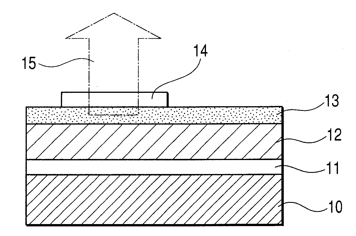
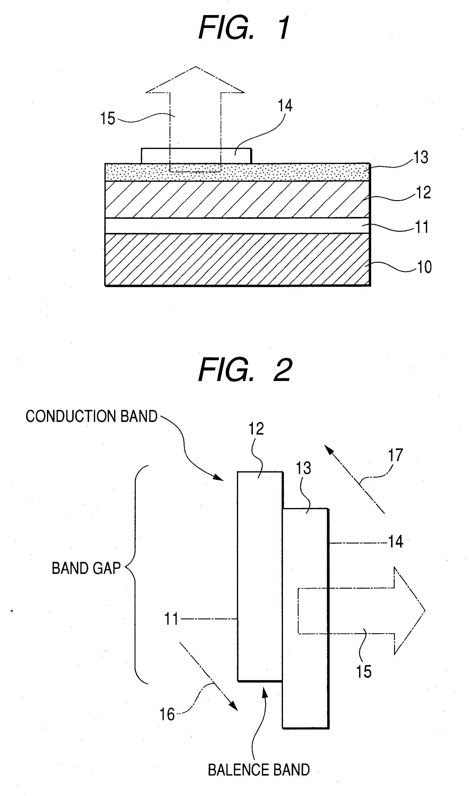
[0034]FIG. 1 is a sectional view showing a schematic constitution of a light emitting device as an embodiment of the present invention.
[0035]As shown in FIG. 1, the light emitting device of this embodiment is obtained by laminating an anode 11 on a substrate 10 and further laminating thereon a semiconductor containing a chalcopyrite (hereinafter referred to as “chalcopyrite semiconductor”) 12, a donor-acceptor pair light emitter 13, and a cathode 14.
[0036]A unit cell of the crystalline structure of a compound represented by a I-III-VI2 type among a large number of existing chalcopyrites is a tetragonal system obtained by stacking two sphalerite structures such as ZnS as a representative example of the group II-VI in the c-axis direction.
[0037]The band structure shows a direct transition type, and selection of constituent elements allows the ...
embodiment 2
[0083]This embodiment is characterized in that a semiconductor containing an oxychalcogenide (hereinafter referred to as “oxychalcogenide semiconductor”) and a light emitting layer in which a compound semiconductor provided with a donor and an acceptor emits light are laminated so as to be adjacent to each other.
[0084]The use of an oxychalcogenide semiconductor instead of the chalcopyrite semiconductor of Embodiment 1 is also one favorable example. With such constitution, a DC drive type light emitting device capable of emitting light with high brightness even at not low temperatures can be obtained.
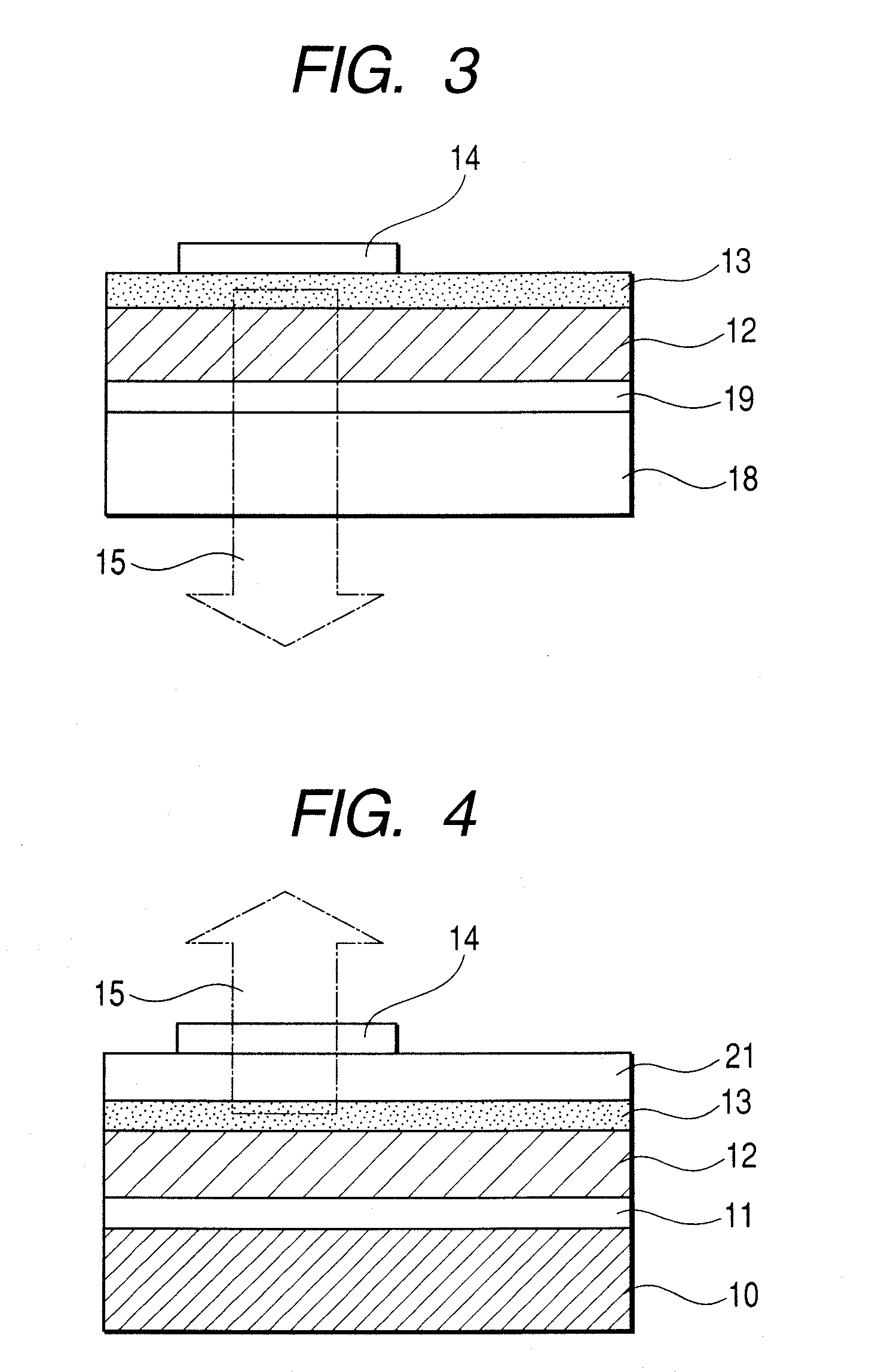
[0085]For example, as shown in FIG. 1, a light emitting device of this embodiment is obtained by laminating the anode 11 on the substrate 10 and laminating thereon the oxychalcogenide semiconductor 12, the donor-acceptor pair light emitter 13, and the cathode 14.
[0086]As described above, the layer constituted of the chalcopyrite semiconductor in Embodiment 1 favorably is of a wide gap se...
example 1
[0111]This example is a first example of the production of a light emitting device having a chalcopyrite semiconductor and a donor-acceptor pair light emitter.
[0112]Pt is formed into a film as the anode 11 on a GaP (100) substrate as the substrate 10. The film, which has a thickness of 100 nm, is formed by using a magnetron sputtering device and a Pt target in a stream of an argon gas under a pressure of 1 Pa at a film deposition rate of 10 nm / min.
[0113]In any subsequent step, a multi-source vacuum deposition device capable of supplying a hydrogen sulfide gas and provided with a resistance heating evaporation source and an electron gun evaporation source is used.
[0114]First, the temperatures of the resistance heating evaporation sources of Cu, Al, and S for obtaining CuAlS2 of the chalcopyrite semiconductor 12 are set to 1,000° C., 1,100° C., and 60° C., respectively.
[0115]Then, the substrate temperature is kept at 600° C., and deposition is conducted to have a thickness of 1 μm in ...
PUM
 Abstract
Description
Claims
Application Information