Transistor device and method

a technology of transistors and transistors, applied in the field of transistor devices and methods, can solve the problems of not significant performance advancement, all the above mentioned methods of enhancement have failed to meet the requirement of a 15 nm si cmos node, and limitations concerning the

Active Publication Date: 2009-05-28
THE BOARD OF TRUSTEES OF THE UNIV OF ILLINOIS
View PDF8 Cites 55 Cited by
  • Summary
  • Abstract
  • Description
  • Claims
  • Application Information

AI Technical Summary

Benefits of technology

[0007]An aspect of the invention relates to a field-effect transistor device, including: a semiconductor heterostructure comprising, in a vertically stacked configuration, a semiconductor gate layer between semiconductor source and drain layers, said layers being separated by heterosteps; said gate layer having a thickness of less than about 100 Angstroms; and source, gate, and drain electrodes respectively coupled with said source, gate, and drain layers. As will be described further herein, separation of the gate by heterosteps, rather than an oxide layer, has very substantial advantages.

Problems solved by technology

Based on silicon metal oxide semiconductor field effect transistor (Si MOSFET) transistor scaling and the so-called research roadmap, the 15 nm node (physical gate length, <7 nm) of Si complementary metal oxide semiconductor (CMOS) will reach a fundamental limitation and will have no significant performance advancement over the larger 22 nm node version due to limitations of mobility and sheet carrier density.
However, all the above mentioned methods of enhancement have failed to meet the requirement of a 15 nm Si CMOS node.
There are numerous issues and limitations concerning the FET, related to breakdown voltage, output conductance, and gate leakage current due to tunneling through the thin gate oxide.

Method used


Image

  • Transistor device and method
  • Transistor device and method
  • Transistor device and method

Examples


Embodiment Construction

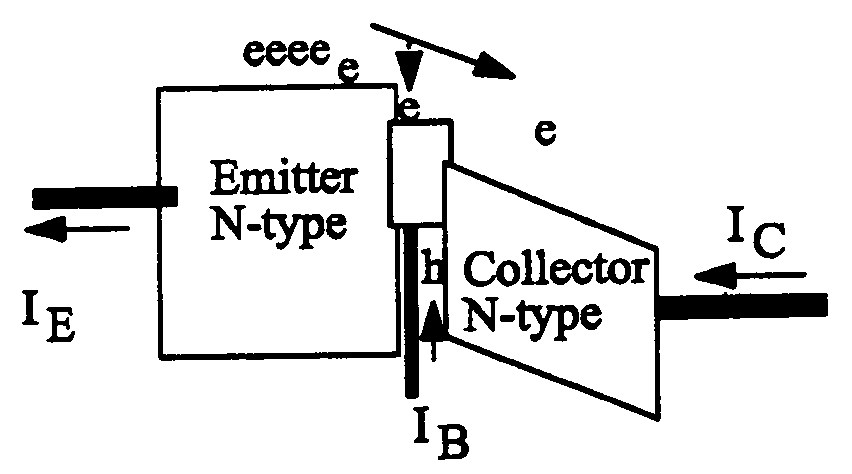
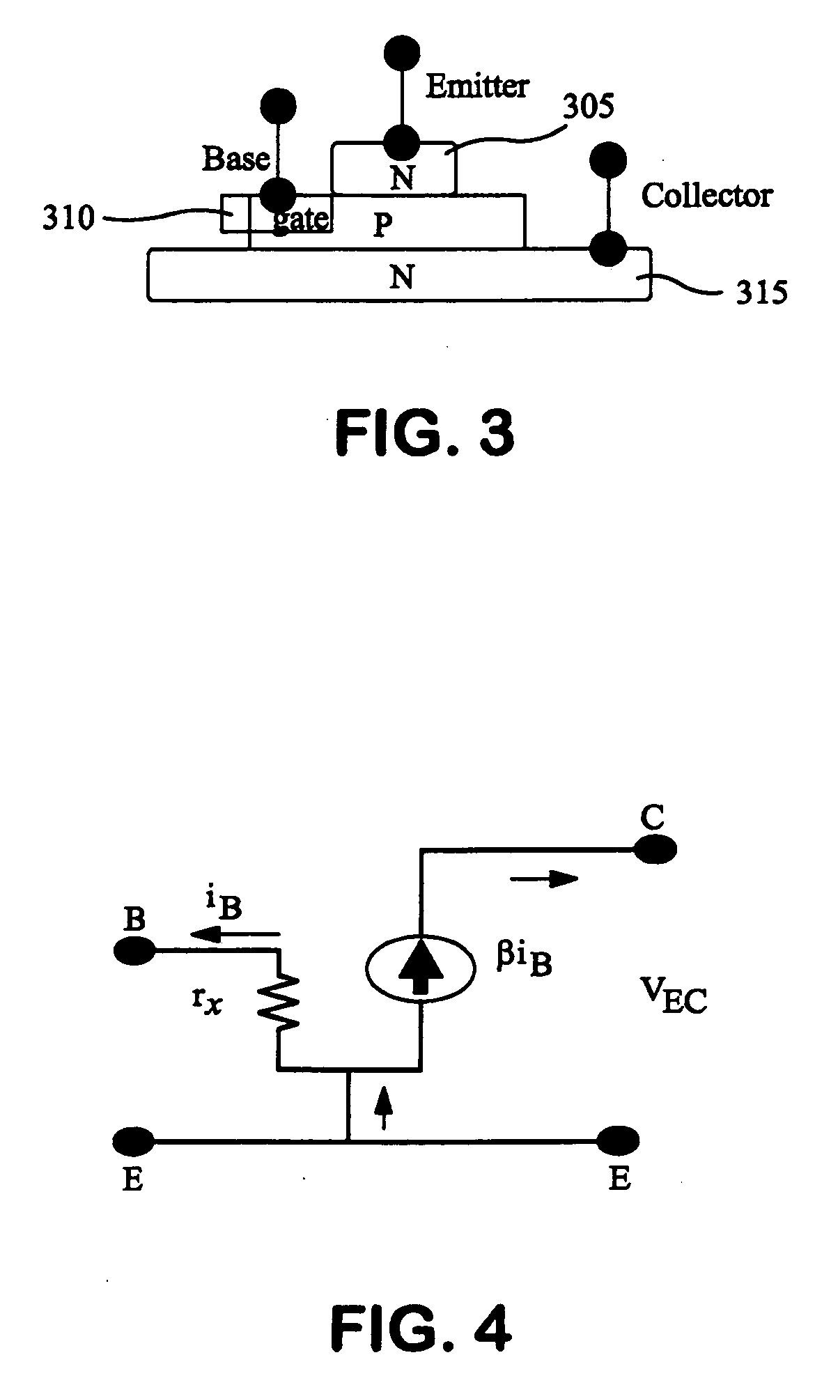
[0021]In accordance with an aspect hereof, an improved FET lies in the implementation of a vertical HFET evolving from an HBT in which there is provided, inter alia, an ultra thin base layer, almost complete transfer of emitter current to the collector with little or no base “loss” or recombination. The HBT ceases functioning as a classical bipolar transistor, and substantially crosses over to functioning as a field effect “transistor”, i.e., as a majority carrier (unipolar) device, Among the objectives hereof are establishing a technique and device which constitute an “HBT” version of a vertical FET, and employing to advantage the fact that, with this approach, extremely small dimensions can be realized between the source and drain (and, in, addition useful heterojunction energy gap steps can be incorporated in the layer stacking from emitter-source to collector-drain).

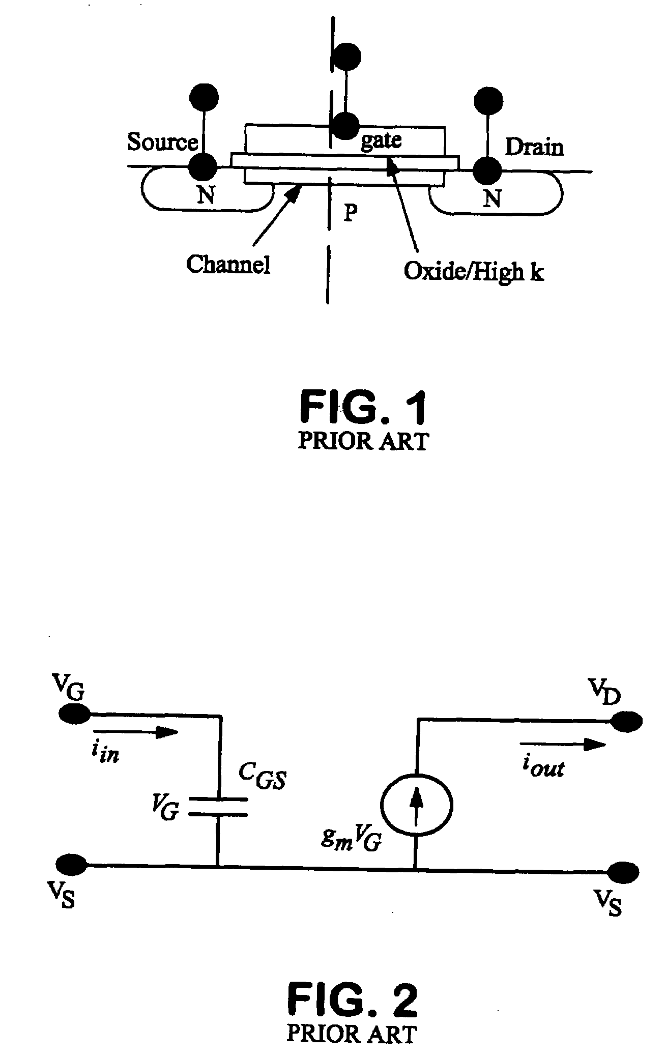
[0022]It can be observed that a conventional FET has another technological limitation; namely, the weakness of sta...


PUM


Abstract

A field-effect transistor device, including: a semiconductor heterostructure comprising, in a vertically stacked configuration, a semiconductor gate layer between semiconductor source and drain layers, the layers being separated by heterosteps; the gate layer having a thickness of less than about 100 Angstroms; and source, gate, and drain electrodes respectively coupled with said source, gate, and drain layers. Separation of the gate by heterosteps, rather than an oxide layer, has very substantial advantages.

Description

PRIORITY CLAIM[0001]Priority is claimed from U.S. Provisional Patent Application No. 60 / 998,651, filed Oct. 12, 2007, and said U.S. Provisional Patent Application is incorporated herein by reference.FIELD OF THE INVENTION[0002]This invention relates to transistor devices and methods, including improvements in field-effect transistor devices and methods and heterojunction bipolar transistor devices and methods.BACKGROUND OF THE INVENTION[0003]Based on silicon metal oxide semiconductor field effect transistor (Si MOSFET) transistor scaling and the so-called research roadmap, the 15 nm node (physical gate length, <7 nm) of Si complementary metal oxide semiconductor (CMOS) will reach a fundamental limitation and will have no significant performance advancement over the larger 22 nm node version due to limitations of mobility and sheet carrier density. To improve the n-MOSFET performance beyond the 15 nm node requires an electron mobility >2000 cm2N-s with a sheet electron density ...

Claims


Application Information

Patent Timeline
Patent Type & Authority Applications(United States)
IPC IPC(8): H03F3/04H01L29/66H01L21/331
CPCH01L29/1004H01L29/7371H01L29/205H01L29/2003
Inventor FENG, MILTONHOLONYAK, JR., NICK
Owner THE BOARD OF TRUSTEES OF THE UNIV OF ILLINOIS
Why Eureka
Try Eureka