sled

Active Publication Date: 2005-07-28
EXALOS
View PDF4 Cites 15 Cited by
  • Summary
  • Abstract
  • Description
  • Claims
  • Application Information

AI Technical Summary

Benefits of technology

[0006] It is an object of the present invention to provide a superluminescent light emitting diode which overcomes disadvantages of prior art superluminescent light emitting diodes a

Problems solved by technology

However, the tilted waveguide or other means of achieving non-perpendicular end

Method used


Image

  • sled
  • sled
  • sled

Examples


Embodiment Construction

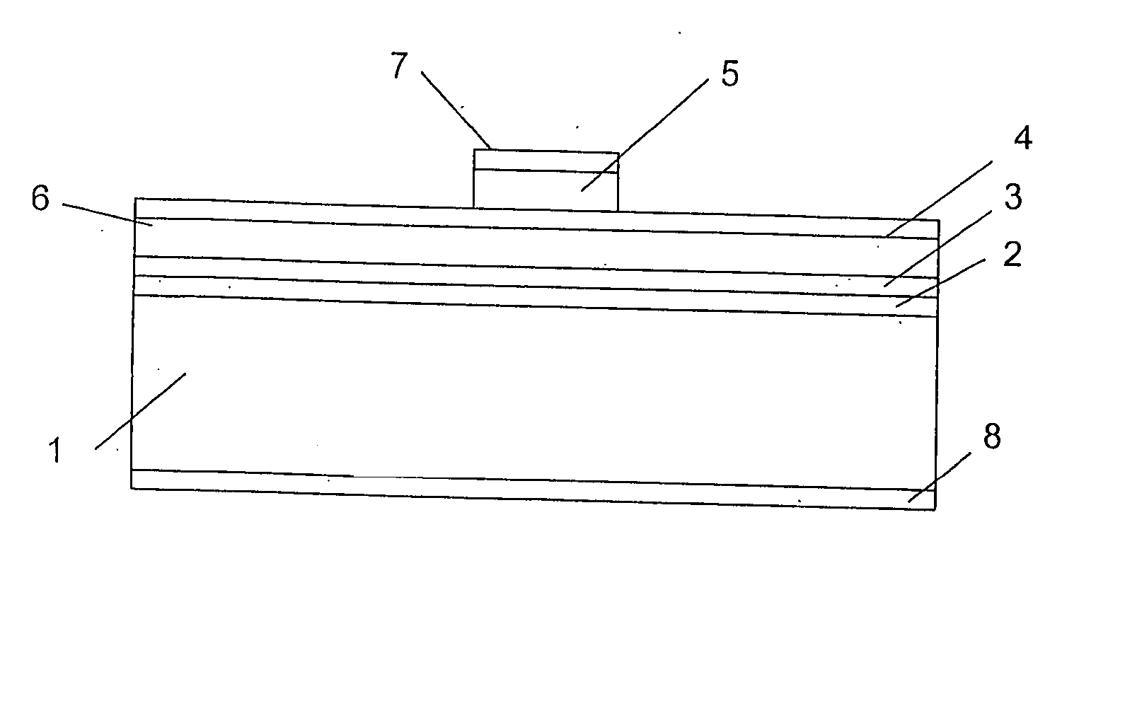
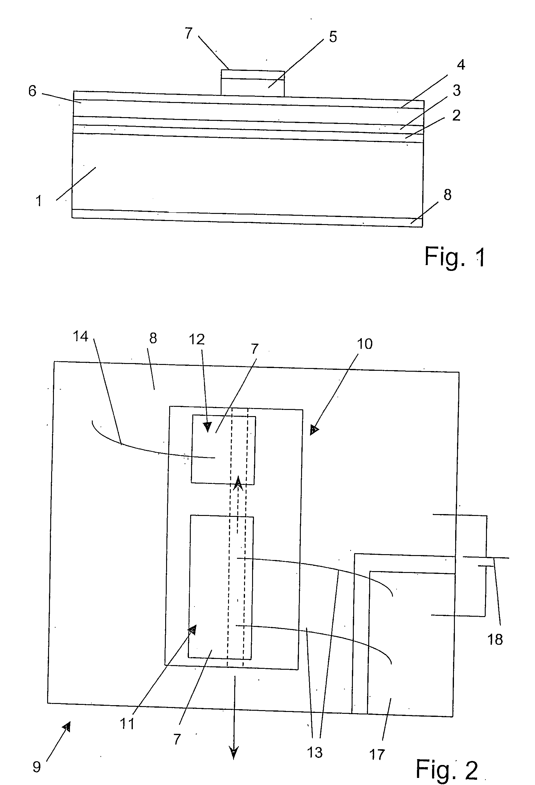
[0019] The device schematically shown in FIG. 1 comprises a semiconductor heterostructure including a GaAs substrate 1. The substrate comprises an Si-doped (the Si doping here being an n-doping) InGaP semiconductor cladding layer 2. On top of the Si-doped cladding layer, a layered structure forming a PN-junction is placed. In the shown embodiment, the PN-junction is formed by an undoped InGaAsP ‘bulk’ structure layer 6, between an Si-doped InGaAsP cladding layer 3 and a Zn-doped (the Zn-doping being a p-doping) InGaAsP cladding layer 4. The layered structure is covered by a Zn-doped InGaP cladding layer 5. The indexes of refraction of the n-doped and the p-doped cladding layers 3, 4 are higher than the index of refraction of the active ‘bulk’ layer 6, so that a waveguide is formed for light generated in the PN junction upon injection of a current. Lateral confinement is achieved by a ridge waveguide structure (weakly index guided structure). For injecting a current, the device compr...


PUM


Abstract

A non-lasing superluminescent light emitting diode (SLED) comprises a semiconductor heterostructure forming a PN junction and a waveguide defining an optical beam path. The heterostructure includes a gain region and an absorber region in series with the gain region in the optical beam path. A voltage is applied to the PN junction in the gain region by first contact means, so that light emission from the active region and along the optical beam path is produced. According to the invention, second contact means are provided, contacting the PN junction in the absorber region and operable to remove charge carriers generated by absorption in the absorber region. The second contact means are not connected to a voltage source, but to a charge carrier reservoir such as a metal surface. According to a preferred embodiment, the two end facets of the waveguide are perpendicular to the optical beam path.

Description

FIELD OF THE INVENTION [0001] This invention is in the field of broadband light sources. It more particularly relates to a superluminescent light emitting diode (SLED) with a gain region and an absorber region. BACKGROUND OF THE INVENTION [0002] Superluminescent light emitting diodes (SLEDs) are diodes that, when biased in the forward direction, become optically active and generate amplified spontaneous emission over a wide range of wavelengths. In contrast to laser diodes, there is not sufficient feedback to achieve lasing action (“lasing” here is used to describe the function principle of a laser, i.e. to generate, by a feedback, stimulated emission in a gain medium pumped to provide population inversion and placed in a cavity providing the feedback, resulting in coherent radiation). This is usually achieved by the joint action of a tilted waveguide in which the generated radiation is guided and anti-reflection coated end facets. A tilted waveguide in this context is a waveguide w...

Claims


Application Information

Patent Timeline
IPC IPC(8): H01L33/00
CPCH01L33/0045
Inventor VELEZ, CHRISTIANREZZONICO, RAFFAELE
Owner EXALOS
Why Eureka
Try Eureka