Conductive pattern forming ink, conductive pattern, and wiring substrate

a technology of conductive pattern and conductive pattern, which is applied in the direction of conductive layer on insulating support, ink, non-conductive material with dispersed conductive material, etc., can solve the problems of fine wiring lines and narrow pitches, densified circuit substrates, and hardly satisfying demand, etc., to achieve excellent discharge properties of droplets, high reliability, and high reliability

Inactive Publication Date: 2009-06-11
SEIKO EPSON CORP
View PDF7 Cites 0 Cited by
  • Summary
  • Abstract
  • Description
  • Claims
  • Application Information

AI Technical Summary

Benefits of technology

[0011]An advantage of the present invention is to provide a conductive pattern forming ink that can prevent the occurrence of cracks and disconnections in a formed conductive pattern, a conductive pattern exhibiting high reliability, and a wiring substrate having the conductive pattern and exhibiting high reliability.
[0012]Such advantage is achieved by the following aspects.
[0013]According to a first aspect of the invention, a conductive pattern forming ink for forming a conductive pattern on a substrate by a droplet discharge method, includes: metal particles; an aqueous dispersion medium in which the metal particles are dispersed; galactitol; and a polyglycero...

Problems solved by technology

The screen printing, however, is disadvantageous in that it is difficult to form fine wiring lines and achieve narrow pitches, and thus hardly satisfies the demand in recent years for highly densified circuit substrates with miniaturized wiring lines (e.g., wiring lines having a line width of 60 μm or less) having a narrow pitch.
In this regard, a related art conductive pattern forming ink has a problem in that conductive fine particles are separated out from the ink for forming a conductive pattern due to volatilization of its dispersion medium around a droplet discharge portion of a droplet discharge head (ink-jet head) during a discharge waiting time and a long time continuing discharge.
The deposited conductive fine particles around the droplet discharge portion cause changing the path...

Method used


Image

  • Conductive pattern forming ink, conductive pattern, and wiring substrate
  • Conductive pattern forming ink, conductive pattern, and wiring substrate
  • Conductive pattern forming ink, conductive pattern, and wiring substrate

Examples


first embodiment

Conductive Pattern Forming Ink

[0048]A conductive pattern forming ink according to a first embodiment of the invention is used for forming a conductive pattern on a substrate, especially used for forming a conductive pattern by a droplet discharge method.

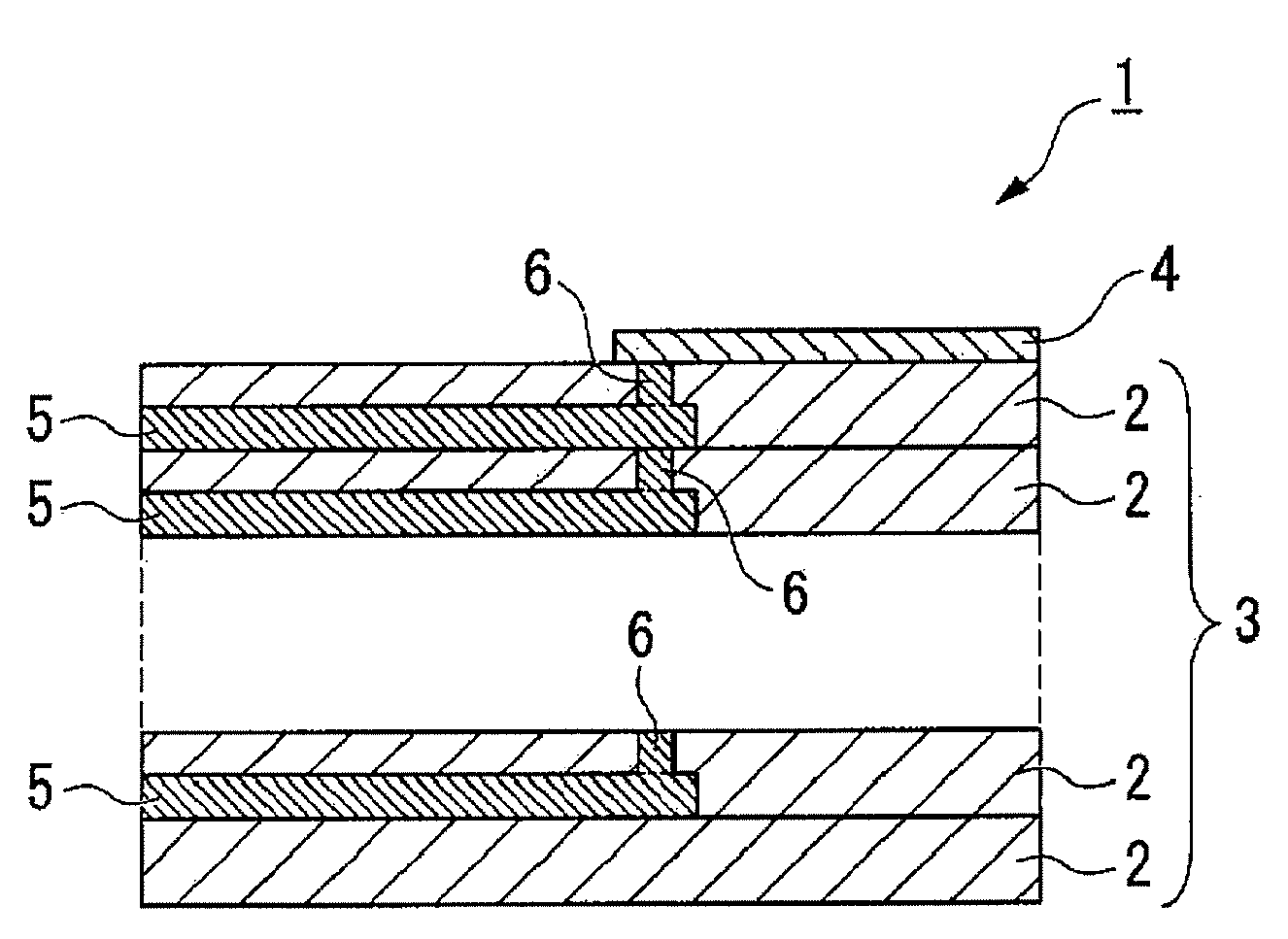
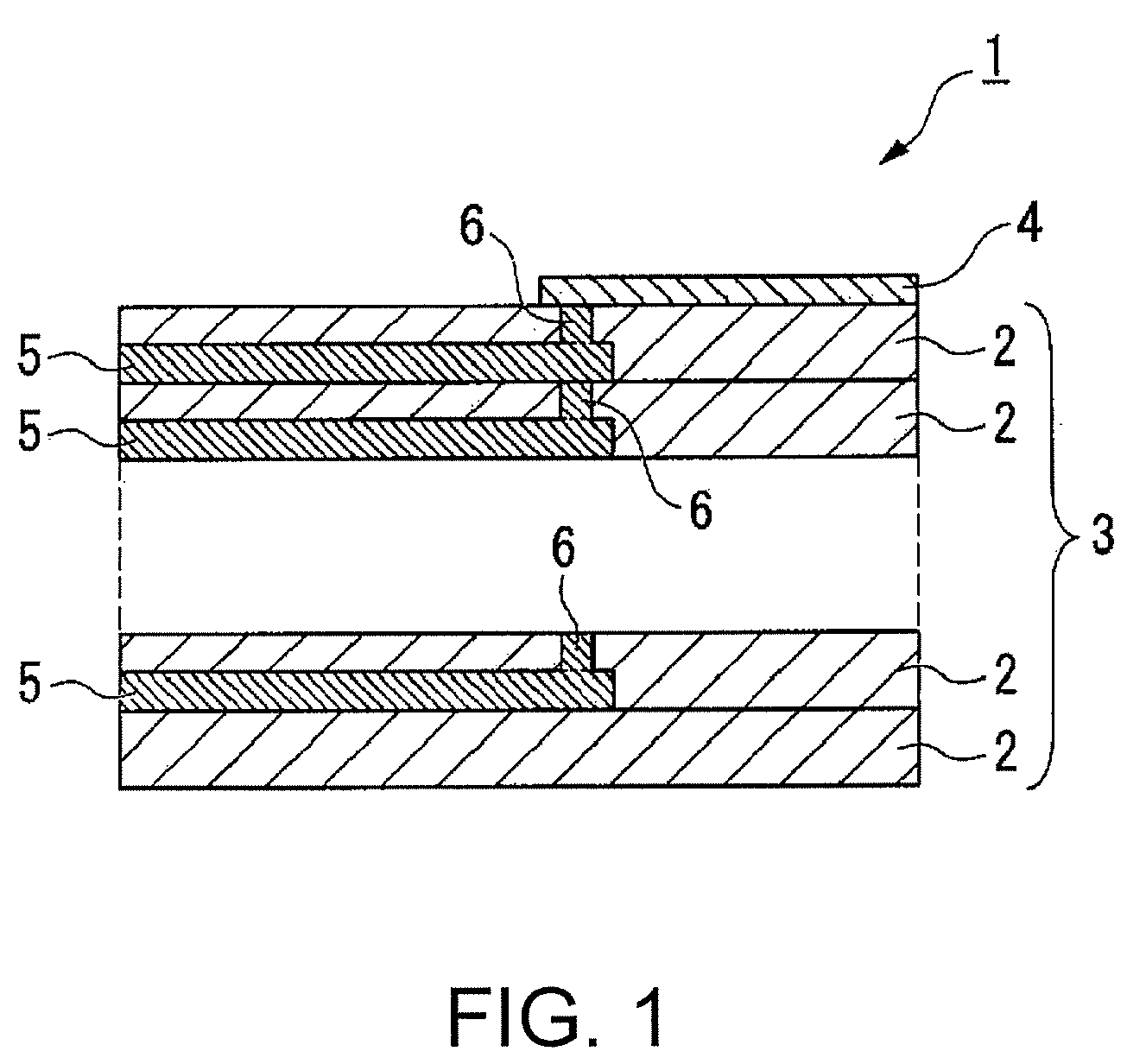
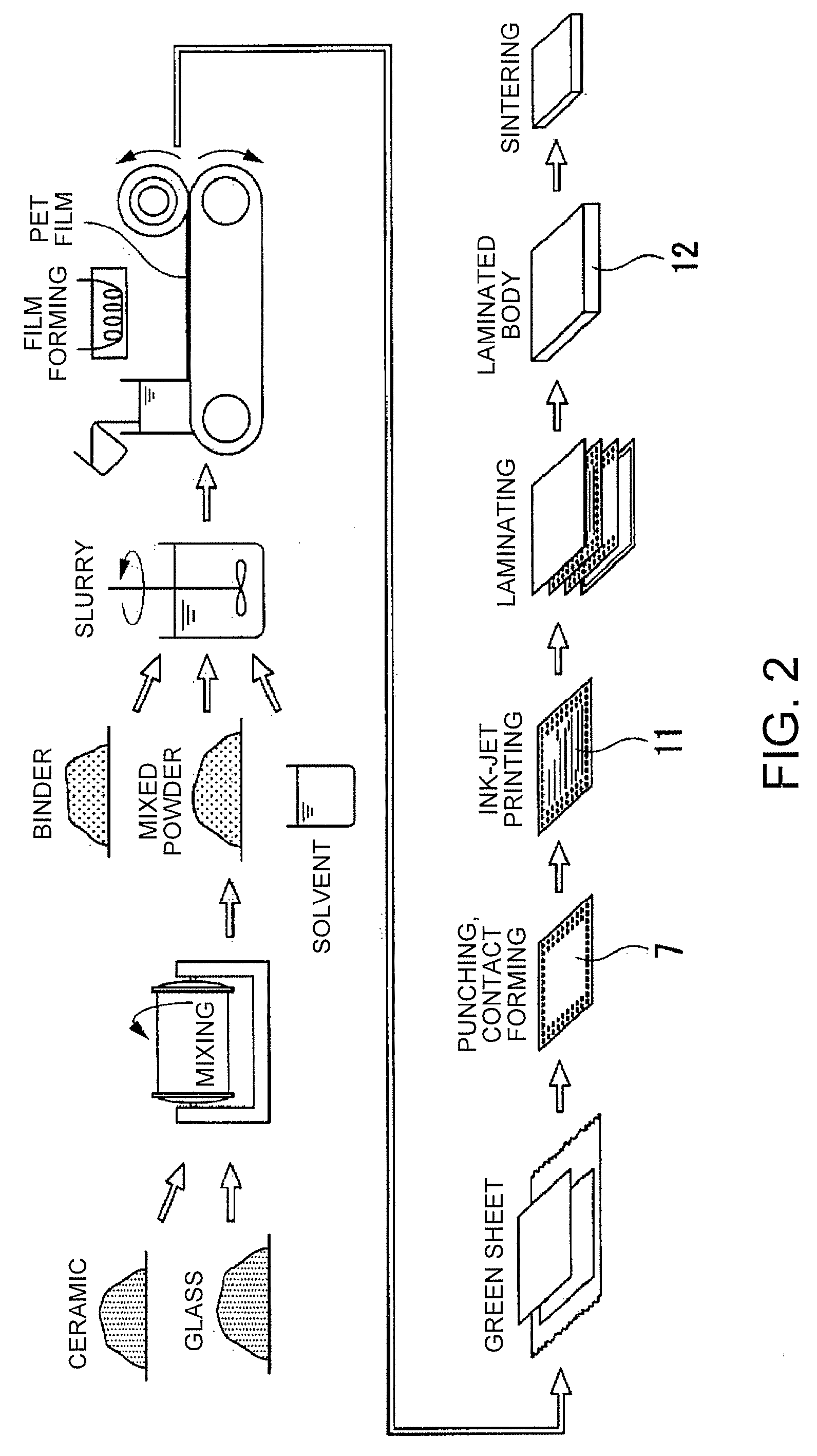
[0049]Any substrate may be used as a substrate on which a conductive pattern is formed. However, a ceramic substrate mainly made of ceramic is employed as the substrate in the embodiment. Further, the first embodiment will be explained by exemplifying a case where the conductive pattern forming ink is applied to a ceramic formed body (a ceramic green sheet) made of ceramic and a material containing a binder and having a sheet-like shape. Here, the ceramic formed body and the ink applied to the ceramic formed body undergo a sintering step as described later so as to be a ceramic substrate and a conductive pattern respectively.

[0050]The conductive pattern forming ink will now be descried. In the embodiment, a case using a dispersion li...

second embodiment

Method for Producing Conductive Pattern Forming Ink

[0120]An example of a method for producing a conductive pattern forming ink such as the ink described above will now be described as a second embodiment of the invention.

[0121]In the second embodiment, the conductive pattern forming ink is a colloidal liquid obtained by dispersing silver colloidal particles in an aqueous dispersion medium.

[0122]In producing a conductive pattern forming ink, an aqueous solution in which a dispersant and a reducing agent are dissolved is first prepared.

[0123]The dispersant is preferably blended in such amount that a molar ratio between silver of silver salt such as silver nitrate which is a starting substance and the dispersant is set to be about 1:1 to about 1:100. If the molar ratio of the dispersant with respect to silver salt is increased, a particle diameter of the silver particles is decreased. Therefore, contact points between the particles in the formed conductive pattern are increased, being ...

third embodiment

Conductive Pattern

[0147]A conductive pattern according to a third embodiment of the invention will now be described.

[0148]The conductive pattern is formed by applying the ink described above on the ceramic formed body and then heating the ceramic formed body so as to have a thin film shape. On the conductive pattern, the silver particles are bonded to each other. The silver particles are bonded to each other with no space therebetween at least on the surface of the conductive pattern.

[0149]Especially, the conductive pattern is formed by using the conductive pattern forming ink of the first embodiment, so that disconnection caused by discharge defects, contact between the conductive patterns that are adjacent to each other, and the like are prevented. Accordingly, the conductive pattern is homogenized without cracks and disconnections so as to be highly reliable.

[0150]The conductive pattern of the third embodiment is formed such that the ink described above is applied on the ceramic ...


PUM

PropertyMeasurementUnit
Acidityaaaaaaaaaa
Electrical conductoraaaaaaaaaa

Abstract

A conductive pattern forming ink for forming a conductive pattern on a substrate by a droplet discharge method includes: metal particles; an aqueous dispersion medium in which the metal particles are dispersed; galactitol; and a polyglycerol compound having a polyglycerol skeleton. In the ink, H shown in the following formula (I) is 0.10 to 0.60;
H=OH(A)Mw(A)X(A)+OH(B)Mw(B)X(B)Formula(I)
where OH(A) represents an average number of hydroxyl groups in one molecule of the polyglycerol compound, Mw(A) represents a weight-average molecular weight of the polyglycerol compound, X(A) represents a content of the polyglycerol compound in the conductive pattern forming ink in weight percent; and OH(B) represents a number of hydroxyl groups in one molecule of the galactitol, Mw(B) represents a molecular weight of the galactitol, and X(B) represents a content of the galactitol in the conductive pattern forming ink in weight percent.

Description

[0001]The entire disclosure of Japanese Patent Application No. 2007-319018, filed Dec. 10, 2007 is expressly incorporated by reference herein.BACKGROUND[0002]1. Technical Field[0003]The present invention relates to a conductive pattern forming ink, a conductive pattern, and a wiring substrate.[0004]2. Related Art[0005]Ceramic circuit substrates are widely used as circuit substrates (wiring substrates) on which electronic components are mounted. The ceramic circuit substrates are substrates made of ceramic (ceramic-substrates) on which wiring lines made of metallic materials are provided. Such ceramic circuit substrates are advantageous in that internal components are formed in a multiple-layer manner and finished dimensions are stable because the ceramic constituting the substrates (ceramic substrates) are multifunctional materials.[0006]The ceramic circuit substrates are manufactured as follows. A composition including metal particles is provided on a ceramic formed body made of a ...

Claims


Application Information

Patent Timeline
IPC IPC(8): H05K1/09C08K5/053C08K5/09C08K5/36C09D11/00H01B1/22H01B5/14H05K3/10
CPCC09D11/326C09D11/52H05K1/0306H05K2203/1131H05K3/125H05K3/4611H05K3/4629H05K1/092Y10S977/775Y10S977/773Y10S977/788Y10S977/777
Inventor TOYODA, NAOYUKI
Owner SEIKO EPSON CORP
Why Eureka
Try Eureka