Electron beam measurement apparatus

a technology of electromagnetic radiation and measurement apparatus, applied in the direction of instruments, semiconductor/solid-state device testing/measurement, image enhancement, etc., can solve the problem of unclear how to measure a sampl

Active Publication Date: 2009-06-11
HITACHI HIGH-TECH CORP
View PDF4 Cites 5 Cited by
  • Summary
  • Abstract
  • Description
  • Claims
  • Application Information

AI Technical Summary

Benefits of technology

[0023]According to the present invention, it is possible to realize an electron beam measurement technique capable of measuring the shape or size of a portion of a pattern delineated on a sample by a multi-exposure method or detecting a defect or the like.

Problems solved by technology

That is, it has been unclear how to measure a sample subjected to a multi-exposure scheme and having a pattern that includes portions having shapes different from each other in a vertical direction.

Method used


Image

  • Electron beam measurement apparatus
  • Electron beam measurement apparatus
  • Electron beam measurement apparatus

Examples


first embodiment

[0036]First, a basic configuration of an electron beam measurement apparatus according to the present invention will be described.

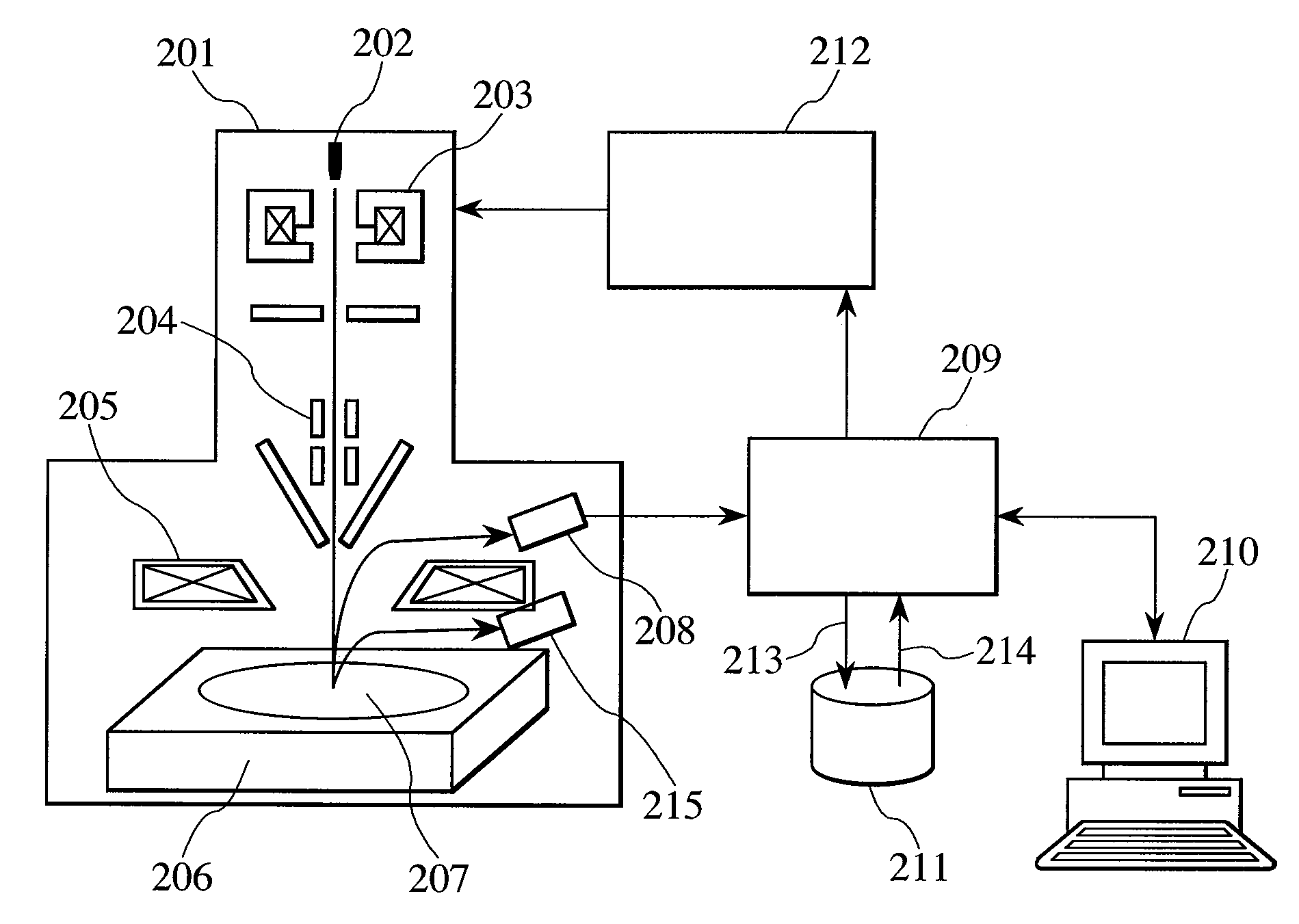
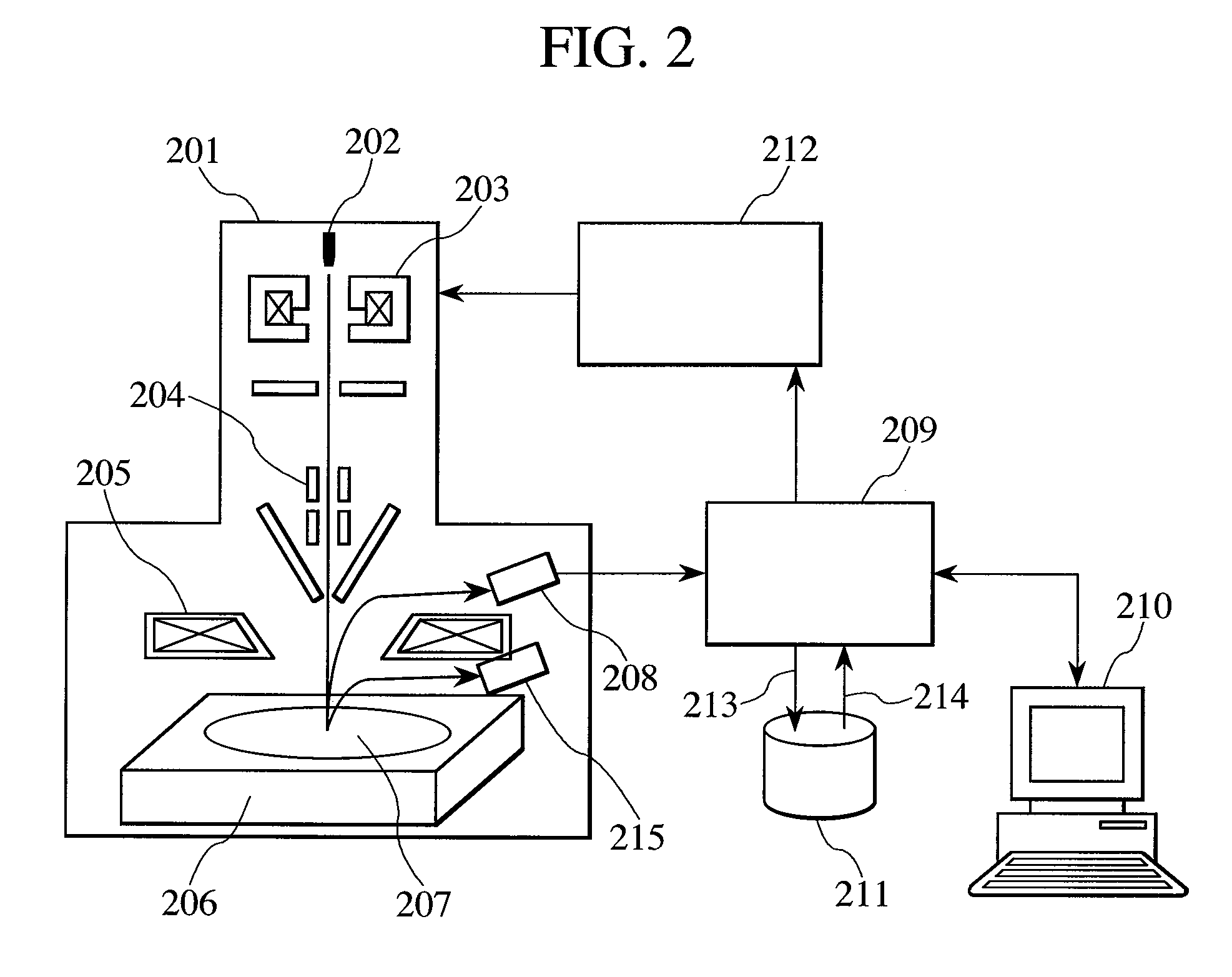
[0037]FIG. 2 is a diagram showing the basic configuration of the electron beam measurement apparatus according to the present invention. The electron beam measurement apparatus has an electron optical system 201, a secondary electron detector 208, a reflective electron detector 215, a computing unit 209, a display unit 210, a storage unit 211, and an electron optical system controller 212. The electron optical system 201 uses a condenser lens 203, a deflector 204 and an objective lens 205 to irradiate a sample (wafer) 207 placed on a stage 206 with an electron beam emitted by an electron gun 202 and scan the sample. The secondary electron detector 208 is adapted to detect the intensity of a charged particle (secondary electron) secondarily generated from the sample 207 by the irradiation of the electron beam. The reflective electron detector 215 is adapte...

second embodiment

[0048]FIG. 5 is a flowchart of the measurement according to a second embodiment of the present invention. In the measurement shown in FIG. 5, after an SEM image is acquired, patterns are classified into groups by comparing the SEM image with design data, in step 501. In the pattern (shown in FIG. 9) having lines and spaces which are alternately arranged, matching of the pattern may be performed with a single pitch shifted. This measurement method shown in FIG. 5 is suitable for a logic LSI having a complex pattern. It can be considered that a combination of this measurement method shown in FIG. 5 with the classification method based on the brightness in the first embodiment is effective.

[0049]According to the present embodiment, the contour of a portion of each pattern is detected, and the length of the contour is evaluated, to inspect a hot spot (which is a location at which a defect is likely to occur). As a result, detection sensitivity can be improved in the present embodiment, ...

third embodiment

[0050]FIG. 6 is a flowchart showing a measurement according to a third embodiment of the present invention. In the present embodiment, a plurality of images is used. After the sample is moved to a location defined by coordinates of an area to be imaged, a single SEM image is acquired under a first condition in step 601, and a single SEM image is acquired in step 602 under a second condition different from the first condition. Under the first condition, the number of times of scanning of an observation area is eight. Under the second condition, the number of times of television scanning of the observation area is 32. The reason for acquiring the images under the conditions different from each other is that the intensity of a signal coming from the processed layer is low. Thus, the number of times of the scanning under the second condition is 32 in order to improve a signal-to-noise ratio. The intensity of a signal coming from the hard mask layer is too high when the image acquisition...


PUM


Abstract

The present invention provides an electron beam measurement technique for measuring the shapes or sizes of portions of patterns on a sample, or detecting a defect or the like. An electron beam measurement apparatus has a unit for irradiating the patterns delineated on a substrate by a multi-exposure method, and classifying the patterns in an acquired image into multiple groups according to an exposure history record. The exposure history record is obtained based on brightness of the patterns and a difference between white bands of the patterns.

Description

CLAIM OF PRIORITY[0001]The present application claims priority from Japanese patent application JP 2007-315940, filed on Dec. 6, 2007, the content of which is hereby incorporated by reference into this application.BACKGROUND OF THE INVENTION[0002]The present invention relates to an electron beam measurement technique for measuring the shapes or sizes of portions of patterns on a sample, or detecting a defect or the like.[0003]In recent years, a semiconductor element has been miniaturized, and dimensional control with high accuracy has been demanded. With the miniaturization of the semiconductor element, the wavelength of light used in a lithographic process has been reduced. In the most currently advanced factory, an ArF excimer laser (having a wavelength of 193 nm) is used. In order to miniaturize the semiconductor element, an extreme ultraviolet (EUV) lithography using light with a wavelength of 13 nm is considered as a candidate. However, since the wavelength of light used in the...

Claims


Application Information

Patent Timeline
IPC IPC(8): G21K7/00
CPCG03F7/70541G03F7/70625G03F7/7065G06T7/0006H01L22/12G06T2207/30148H01J2237/221H01J2237/24578H01J2237/2817G06T2207/10056
Inventor SOHDA, YASUNARIHOTTA, SHOJIOKAZAKI, SHINJIFUKUDA, MUNEYUKI
Owner HITACHI HIGH-TECH CORP
Why Eureka
Try Eureka