Composite Passivation Process for Nitride FET

Active Publication Date: 2009-06-11
NORTHROP GRUMMAN SYST CORP
View PDF9 Cites 26 Cited by
  • Summary
  • Abstract
  • Description
  • Claims
  • Application Information

AI Technical Summary

Benefits of technology

[0010]In accordance with the teachings of the present invention, a nitride-based FET device is disclosed that provides reduced electron trapping and gate current leakage. The device includes a relatively thick passivation layer in the access regions of the device to reduce traps caused by device processing and a thin passivation layer below the gate terminal to reduce gate current leakage. The device includes semiconductor device layers deposited on a substrate. A plurality of passivation layers are deposited on the semiconductor device layers, where at least two of the layers are made of a different dielectric material to provide an etch stop. The passivation layers may be ful

Problems solved by technology

However, these devices have had limited performance because they can suffer from electron trapping near the device surface and high gate terminal current leakage.
Dispersion or current collapse caused by electrons trapped at the surface of the semiconductor device near the gate terminal edge reduces the achievable power performance of nitride-based FET devices.
In addition, under high bias conditions, the high electric fields near the gate terminal edge during device operation can cause trap formation and increases dispersion during device operation leading to premature degradation of t

Method used


Image

  • Composite Passivation Process for Nitride FET
  • Composite Passivation Process for Nitride FET
  • Composite Passivation Process for Nitride FET

Examples


Example

[0019]The following discussion of the embodiments of the invention directed to an FET device employing passivation layers where one of the layers acts as an etch stop for a gate terminal of the device is merely exemplary in nature, and is in no way intended to limit the invention or its applications or uses. For example, the present invention is applicable for many different types of FET and other semiconductor devices as will be appreciated by those skilled in the art.

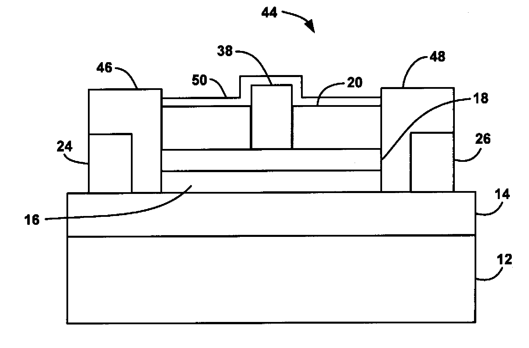
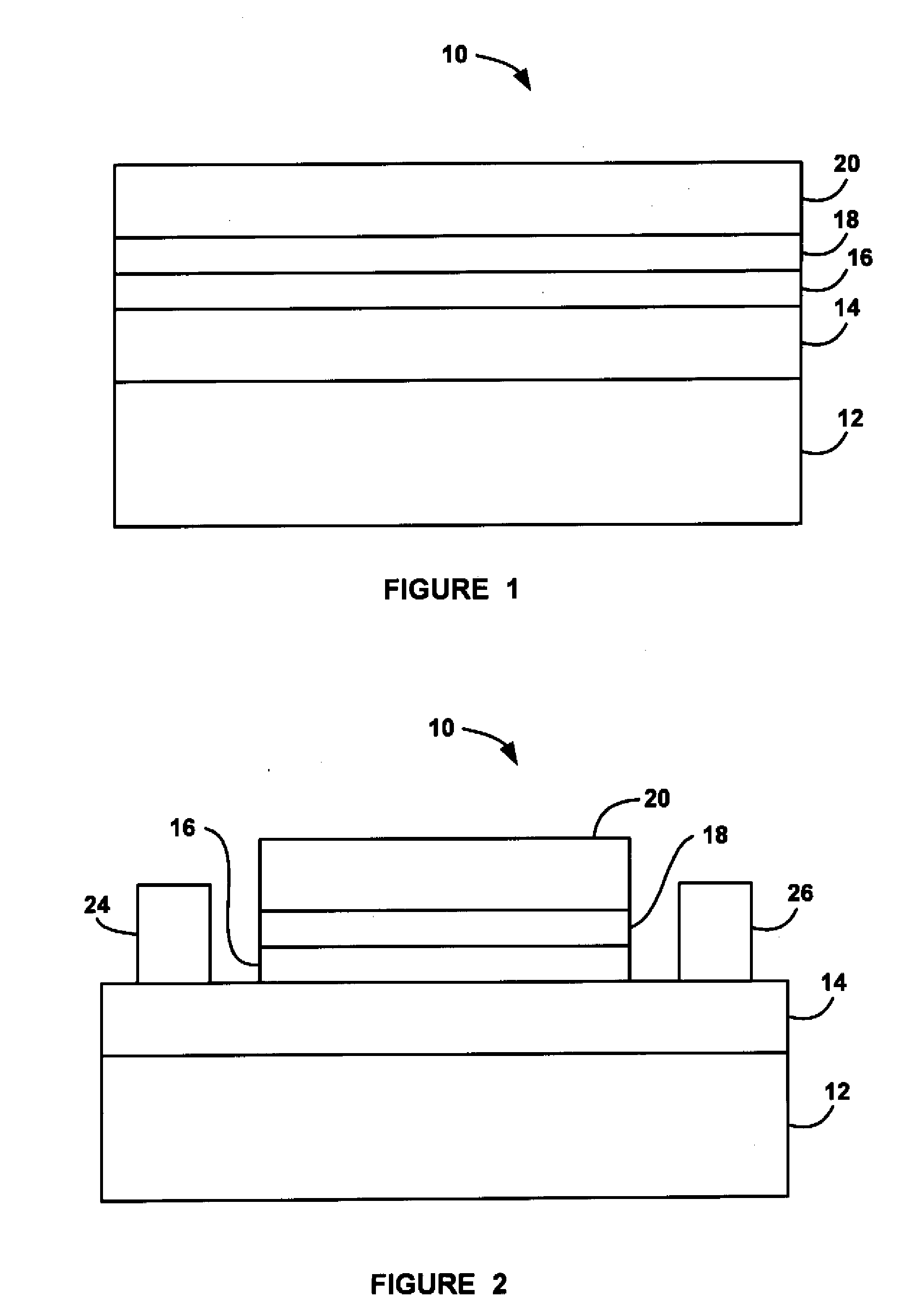
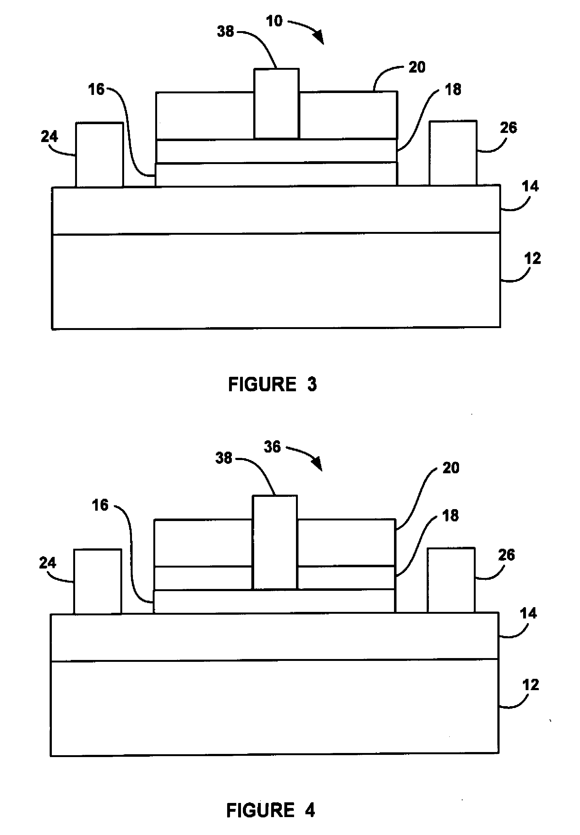
[0020]FIG. 1 is a cross-sectional view of the material profile of a semiconductor device 10, according to an embodiment of the present invention. FIG. 1 is intended to show a partial fabrication step of the device 10, where the device 10 can be any suitable nitride-based field effect transistor (FET) device, such as high electron mobility transistor (HEMT) devices, metal semiconductor field effect transistor (MESFET) devices, metal oxide field effect transistor (MOSFET) devices, metal insulator field effect transistor...


PUM


Abstract

A nitride-based FET device that provides reduced electron trapping and gate current leakage. The device includes a relatively thick passivation layer to reduce traps caused by device processing and a thin passivation layer below the gate terminal to reduce gate current leakage. The device includes semiconductor device layers deposited on a substrate. A plurality of passivation layers are deposited on the semiconductor device layers, where at least two of the layers are made of a different dielectric material to provide an etch stop. One or more of the passivation layers can be removed using the interfaces between the layers as an etch stop so that the distance between the gate terminal and the semiconductor device layers can be tightly controlled, where the distance can be made very thin to increase device performance and reduce gate current leakage.

Description

GOVERNMENT CONTRACT[0001]This invention was made with Government support under Contract No. N00014-05-C-0121 awarded by the Office of Naval Research. The Government may have certain rights in this invention.BACKGROUND OF THE INVENTION[0002]1. Field of the Invention[0003]This invention relates generally to a nitride-based field effect transistor (FET) device employing a plurality of dielectric passivation layers and, more particularly, to a nitride-based FET device including at least two dielectric passivation layers deposited on semiconductor device layers, where two of the passivation layers are made of different materials so that an interface between the layers acts as an etch stop to accurately control the distance between a gate terminal and the semiconductor device layers.[0004]2. Discussion of the Related Art[0005]Due to the wide bandgap and high carrier saturation velocity, nitride-based FET devices are ideal for high frequency and high power applications. However, these devi...

Claims


Application Information

Patent Timeline
IPC IPC(8): H01L21/76
CPCH01L23/3171H01L29/2003H01L29/452H01L29/513H01L29/66568H01L29/7787H01L2924/0002H01L29/78H01L2924/13091H01L2924/13063H01L2924/00
Inventor HEYING, BENJAMINSMORCHKOVA, IOULIAGAMBIN, VINCENTCOFFIE, ROBERT
Owner NORTHROP GRUMMAN SYST CORP
Why Eureka
Try Eureka