Method for manufacturing thin film transistor (TFT) and OLED display having tfts manufactured by the same

a technology of thin film transistors and oled displays, which is applied in the direction of electrical equipment, semiconductor devices, instruments, etc., can solve the problems of non-uniform phenomenon of luminance, low manufacturing efficiency, and low production efficiency, and achieve excellent electrical performance, high carrier mobility, and good stability

Active Publication Date: 2009-06-11
INNOLUX CORP
View PDF7 Cites 26 Cited by
  • Summary
  • Abstract
  • Description
  • Claims
  • Application Information

AI Technical Summary

Benefits of technology

[0005]An objective of the present invention is to provide an OLED display TFT manufacturing method for manufacturing N-type and P-type peripheral circuit TFTs for an OLED display peripheral circuit as well as a switch TFT and driving TFT used in a driving circuit of a display area. By using the method of the present invention, the manufactured per

Problems solved by technology

Not like a silicon wafer used for manufacturing general transistors, the glass substrate suitable for a flat display cannot endure high temperatures, and therefore it is required to use a crystallization technique in which the temperature is lower than the melting temperature of glass substrate.
However, the standard laser crystallization technique has a pro

Method used


Image

  • Method for manufacturing thin film transistor (TFT) and OLED display having tfts manufactured by the same
  • Method for manufacturing thin film transistor (TFT) and OLED display having tfts manufactured by the same
  • Method for manufacturing thin film transistor (TFT) and OLED display having tfts manufactured by the same

Examples


Embodiment Construction

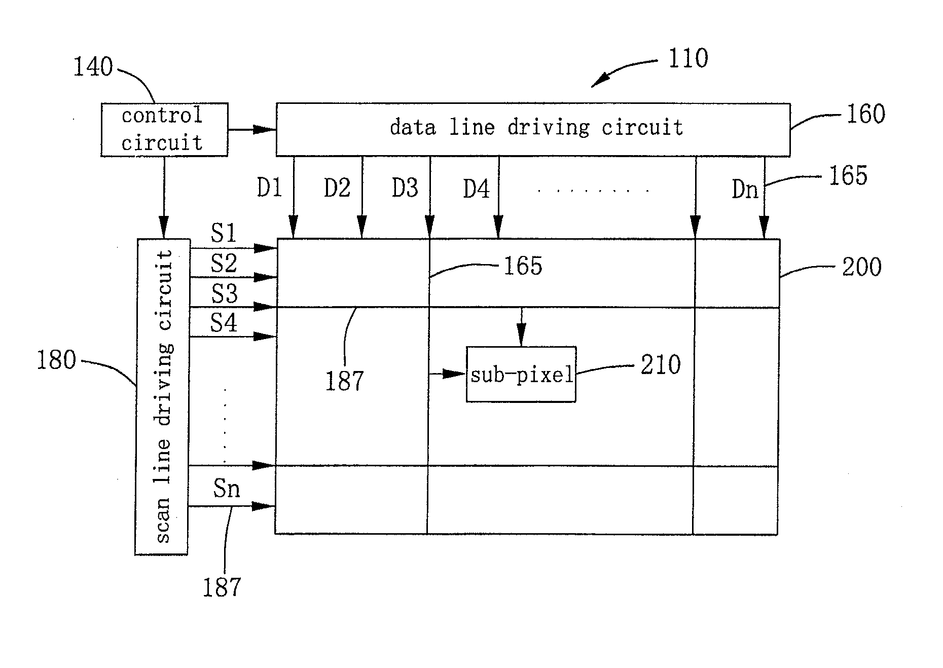
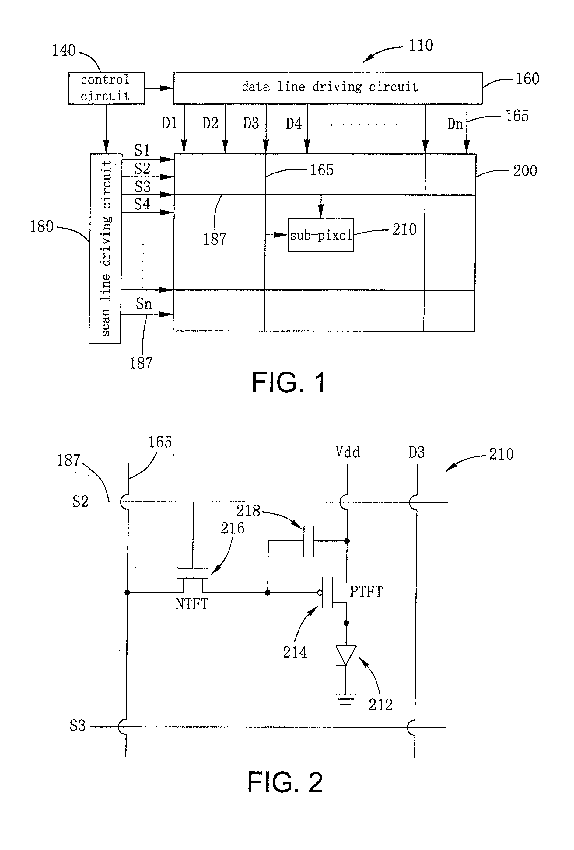
[0016]FIG. 1 is a schematic diagram showing a basic circuit structure of an AMOLED display 110. The OLED display 110 includes a control circuit 140, a data line driving circuit 160, a scan line driving circuit 180 and a display panel 200. The display panel 200 has a plurality of sub-pixels 210. Each sub-pixel 210 is connected with a data line (D1-Dn) 165 and a scan line (S1-Sn) 187 so as to form a matrix. The sub-pixel 210 receives an image data signal from the data line driving circuit 160 via the data line 165 and receives a switch / address signal from the scan line driving circuit 180 via the scan line 187. The data line driving circuit160 and the scan line driving line circuit 180 are controlled by the control circuit 140.

[0017]The sub-pixel can be designed to contain several TFTs. Generally, each sub-pixel comprises at least a driving TFT for driving a light emitting element and a switch TFT for switching the state of the sub-pixel, as shown in FIG. 2. FIG. 2 schematically shows...


PUM


Abstract

An organic light emitting diode (OLED) display and thin film transistor (TFT) manufacturing method thereof are disclosed. According to the present invention, poly-silicon layers for forming active areas of non-driving TFT (e.g. peripheral circuit TFT and switch TFT) and driving TFT used in the OLED display are respectively made by using standard laser crystallization method and non-laser crystallization method or low energy laser crystallization method. Therefore, the peripheral circuit TFT has excellent electrical performance such as high carrier mobility, while the OLED-driving TFT has good stability so that the resultant display can operate with improved luminance uniformity.

Description

TECHNICAL FIELD OF THE INVENTION[0001]The present invention relates to an active matrix organic light emitting diode (AMOLED) display, more particularly, to a method for manufacturing various thin film transistors (TFTs) used in AMOLED displays and an AMOLED display having such TFTs.BACKGROUND OF THE INVENTION[0002]Organic light emitting diodes (OLEDs) have been widely utilized in displays. An AMOLED display uses a driving circuit to drive a light emitting element, i.e. an OLED. The AMOLED driving circuit uses TFTs, including a switch TFT and a driving TFT. The switch TFT, which is implemented by an N-type TFT (NTFT), is used for switching the ON / OFF state of a sub-pixel of the display. The driving TFT, which is implemented by a P-type TFT (PTFT), is used for driving the light emitting element (e.g. an OLED). In addition, a peripheral circuit of the AMOLED display also needs to use NTFT and PTFT. Conventionally, polycrystalline silicon (also referred to as poly-silicon) used in the ...

Claims


Application Information

Patent Timeline
IPC IPC(8): G09G3/30H01L21/84
CPCG09G3/3225G09G2300/0426H01L29/78621H01L27/1237H01L27/3262G09G2300/0439H10K59/1213
Inventor WAN, TE-CHANGLIU, YU-CHUNGLEE, TE-YU
Owner INNOLUX CORP
Why Eureka
Try Eureka