
Memory controller with write data cache and read data cache

a memory controller and write data technology, applied in memory systems, electric digital data processing, instruments, etc., can solve problems such as data hazards, read-after-write hazards, and complication in avoiding hazards, so as to effectively control such a system, avoid data loss, and improve overall performance

Active Publication Date: 2009-06-18
ARM LTD
View PDF14 Cites 97 Cited by
  • Summary
  • Abstract
  • Description
  • Claims
  • Application Information

AI Technical Summary

Benefits of technology

[0014]The separate provision of a write data cache and a read data cache within the memory controller in combination with coherency circuitry for managing coherence between the write data and the read data held within the respective caches and the data stored within the memory enables, an advantageous increase in throughput, provides a good degree of separation between the system side and the memory side of the memory controller, provides a flexible architecture supporting a wide range of memory systems and permits the reordering of access requests in a way which facilitates improved performance and reduces processing bottlenecks.
[0015]In some embodiments the coherency can use the data stored within the read data cache and the write data cache to provide the effect of giving access to the memory when it is in a plurality of different states, e.g. different states each corresponding to the state following a corresponding one of a sequence of write operations. Such behaviour is not possible with a standard cache memory which normally has as an important design objective providing a unified and consistent view of a main memory at one point in time so that coherency issues can be avoided.
[0019]The coherency circuitry can conveniently utilise a hit mask to represent which portions of the read-target data correspond to write data currently stored within the write data cache and which portions do not correspond to any write data currently stored within the write data cache.
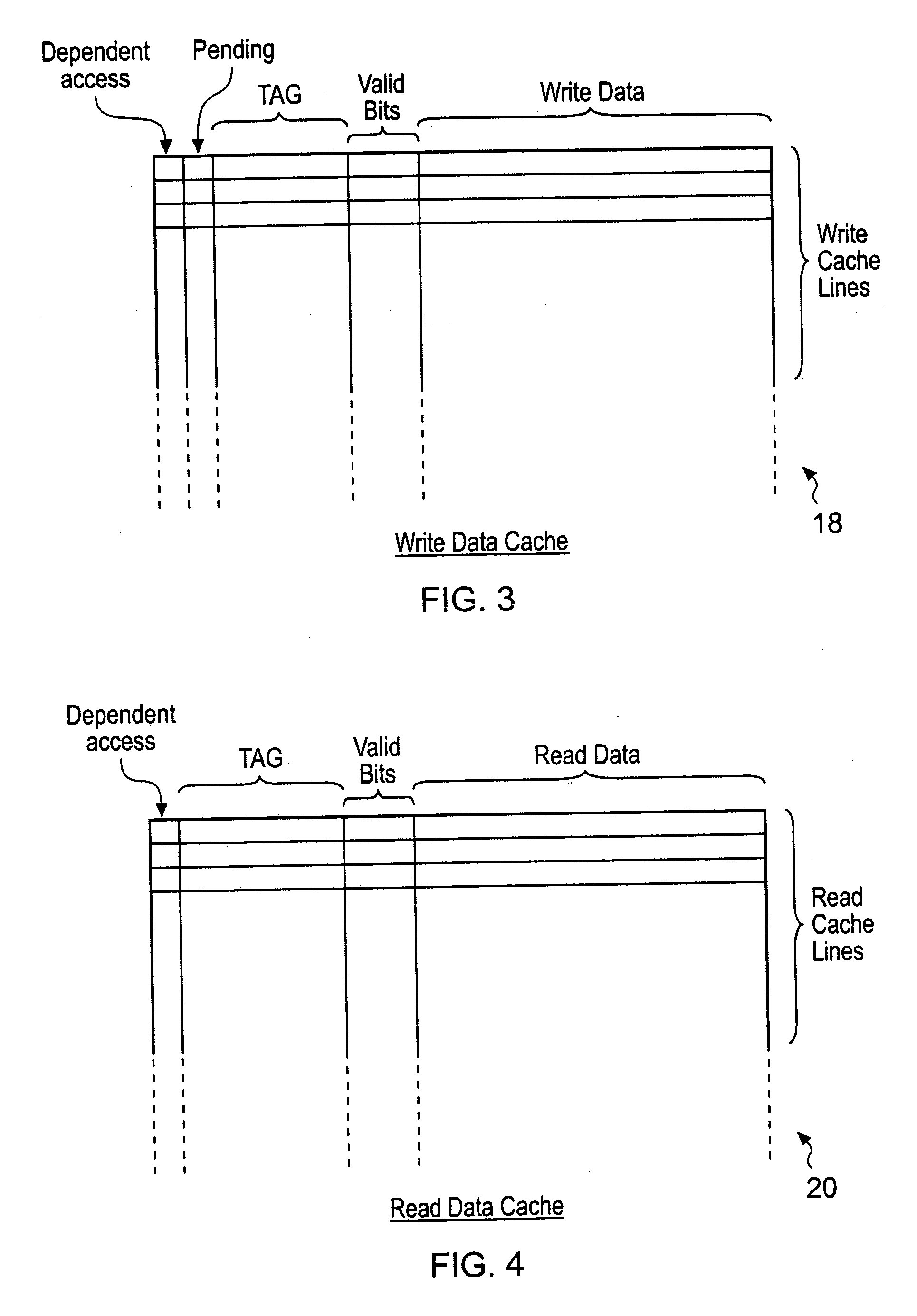
[0022]The decoupling of the system side and the memory side of the memory controller is assisted by the use of valid bits being set to indicate when read cache lines contain valid data fetched from the memory. In this way, the fetching of data from the memory is decoupled from the operation of the system side and yet the system side, is able to respond when valid data has been appropriately fetched.
[0025]The memory controller can buffer write requests and improve throughput by returning a completed response to write requesting circuitry when the write data is stored within the write data cache and before the write data is actually written to the memory.
[0026]In association with the memory controller there may be provided prefetch circuitry which is responsive to access requests received by the memory controller to predict future read requests and to issue corresponding prefetch read requests to the read data cache. Observed behaviour in this way is used to predict future behaviour and spare resource, if any, within the memory controller can be used to prefetch data in a manner seeking to improve overall performance.

Problems solved by technology

One problem which can arise in this context are data hazards such as read-after-write hazards which can be introduced by the reordering of data accesses permitted by interconnect structures.
Reordering is desirable in order to improve throughput, but gives rise to complication in avoiding hazards.
However, this approach has the result that the write accesses incur the full memory latency penalty.
The interface between a memory controller and a memory can often represent a significant bottleneck in the performance of a data processing system.
It is common for memories to be provided off-chip and this can result in an increase in the energy required to make memory accesses and the latency associated with such memory accesses.

Method used


Image

  • Memory controller with write data cache and read data cache
  • Memory controller with write data cache and read data cache
  • Memory controller with write data cache and read data cache

Examples


Embodiment Construction

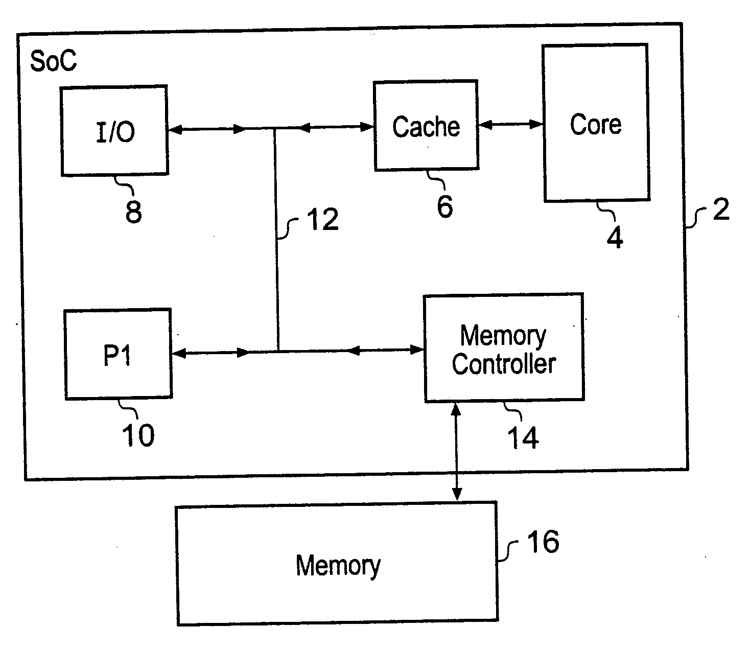
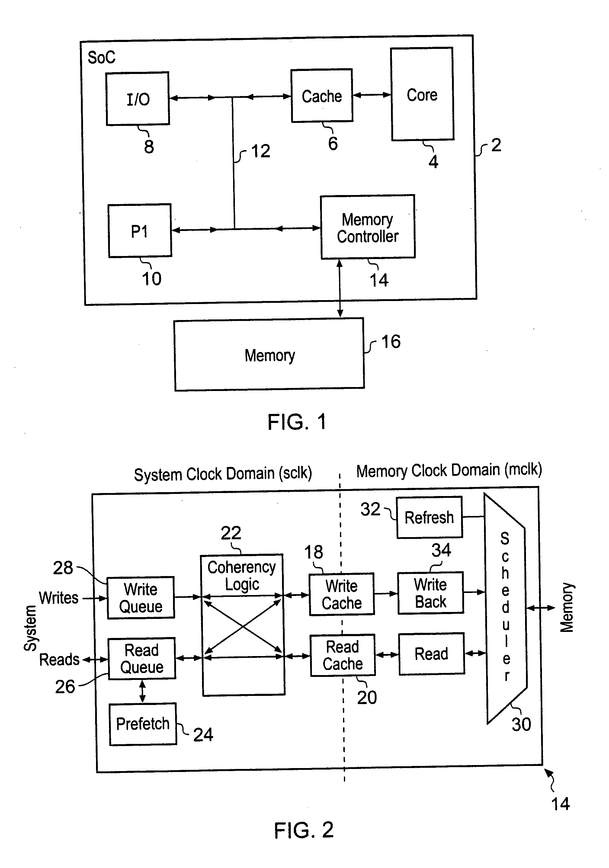
[0050]FIG. 1 illustrates a system-on-chip integrated circuit 2 including a processor core 4, a processor cache memory 6, an input / output functional block 8, a peripheral 10 and a memory controller 14 all connected via an interconnect 12. This interconnect 12 may have the form of an AXM interconnect as previously discussed or may have a different form. The memory controller 14 provides access to an off-chip memory 16, which may have the form of a DRAM, SRAM or other form of memory.

[0051]In operation, the memory controller 14 receives memory access requests, being either read access requests or write access requests, from the various other functional units 4, 6, 8, 10 attached to the interconnect 12. The memory controller 14 also serves to generate appropriate refresh signals that drive the memory 16 as well as performing prefetching operations as will be discussed later. It will be appreciated that the memory controller 14 may be programmable, so as to be able to cope with a variety ...


PUM


Abstract

A memory controller 14 includes a write data cache 18, a read data cache 20 and coherency circuitry 22. The coherency circuitry 22 manages coherency of data between the write data cache 18, the read data cache 20 and data stored within a main memory 16 when servicing read requests and write requests received by the memory controller 14. Write complete signals are issued back to a write requesting circuit as soon as a write request has had its write data stored within the write data cache 18.

Description

BACKGROUND OF THE INVENTION[0001]1. Field of the Invention[0002]This invention relates to the field of memory controllers.[0003]2. Description of the Prior Art[0004]It is known to provide memory controllers which serve the function of generating appropriate signals to perform data accesses (both reads and writes) to memory taking into account the requirements for control signals, setup, timing and other matters required by the memory concerned.[0005]Typical design requirements for memory controllers are the ability to cope with different memory types, the ability to drive periodic refresh, the ability to deal with clock domain crossing and, bus width conversion and to exploit the provision of open pages and access reordering which are possible with some memory configurations in order to increase throughput and / or meet quality-of-service requirements.[0006]It is also known within integrated circuit design to produce so called system-on-chip integrated circuits in which different func...

Claims


Application Information

Patent Timeline
IPC IPC(8): G06F12/00
CPCG06F12/0817
Inventor BRUCE, ALISTAIR CRONE
Owner ARM LTD
Learn More