Sample Holder, Method for Observation and Inspection, and Apparatus for Observation and Inspection

a technology for storing and analyzing samples, applied in material analysis using wave/particle radiation, instruments, nuclear engineering, etc., can solve problems such as inability to improve resolution, difficult to use secondary electrons in imaging samples, and affecting the observation or inspection of samples, so as to achieve high resolution and reduce the amount of samples

Inactive Publication Date: 2009-07-02
JEOL LTD
View PDF2 Cites 82 Cited by
  • Summary
  • Abstract
  • Description
  • Claims
  • Application Information

AI Technical Summary

Benefits of technology

[0013]A sample holder for use in SEM uses a thin film less than 10 nm thick and so secondary electrons can be detected. Consequently, imaging and inspection can be performed at higher resolution. A sample holder for use in TEM permits the distance between thin films to be reduced. Hence, high-resolution imaging and inspection are enabled. The common feature to SEM and TEM sample holders is that a sample containing liquid placed under atmospheric pressure can be observed or inspected after a small amount of the sample is passed through a filter or a medicine is mixed with the sample. In addition, a large number of sample holders can be fabricated because of use of MEMS or nanoimprint technology. It is an object of the present invention to provide such a sample holder. It is another object of the present invention to provide a method of observing or inspecting a sample using such a sample holder. It is a further object of the present invention to provide an apparatus for observing or inspecting a sample using such a sample holder.
[0026]In the present invention, the opening in the frame-like member or the opening portions in the lattice are coated with the film. The relationship between the thickness D of the film and the length D of the outer periphery of the portion of the film that covers the opening in the film or the opening portions in the lattice is given by L / D <200,000. Therefore, if the film is thinned, the film can sufficiently withstand a pressure difference of greater than 1 atm. As a result, in observation or inspection using a primary beam such as in SEM or TEM, high resolution can be obtained.
[0027]Microlithography can be done by forming the film by an MEMS process including silicon nitride or by a nanoimprint process. Therefore, where the sample is passed through a filter or a medicine is mixed into the sample, the amount of sample can be reduced. Furthermore, sample holders can be mass produced by making use of the MEMS process or nanoimprint process.

Problems solved by technology

This hinders observation or inspection of the sample under the condition where it contains moisture.
The thickness of the film is more than 10 nm and so it is difficult to use secondary electrons in imaging the sample.
Hence, it has been impossible to improve the resolution.
However, it has been difficult to obtain 1 atm. pressure resistance.
Furthermore, the sample holder is assembled fully manually, requiring much labor.
Hence, it is impossible to cope with a large number of samples.
Because the sample holder is assembled manually, it is difficult to reduce the spacing between the carbon films.
As a result, there arises the problem that the resolution is deteriorated.
The problem common to SEM and TEM is that a sample of more than 1 milliliter is required when the sample is passed through a filter or a medicine is mixed into the sample.

Method used


Image

  • Sample Holder, Method for Observation and Inspection, and Apparatus for Observation and Inspection
  • Sample Holder, Method for Observation and Inspection, and Apparatus for Observation and Inspection
  • Sample Holder, Method for Observation and Inspection, and Apparatus for Observation and Inspection

Examples


embodiment 1

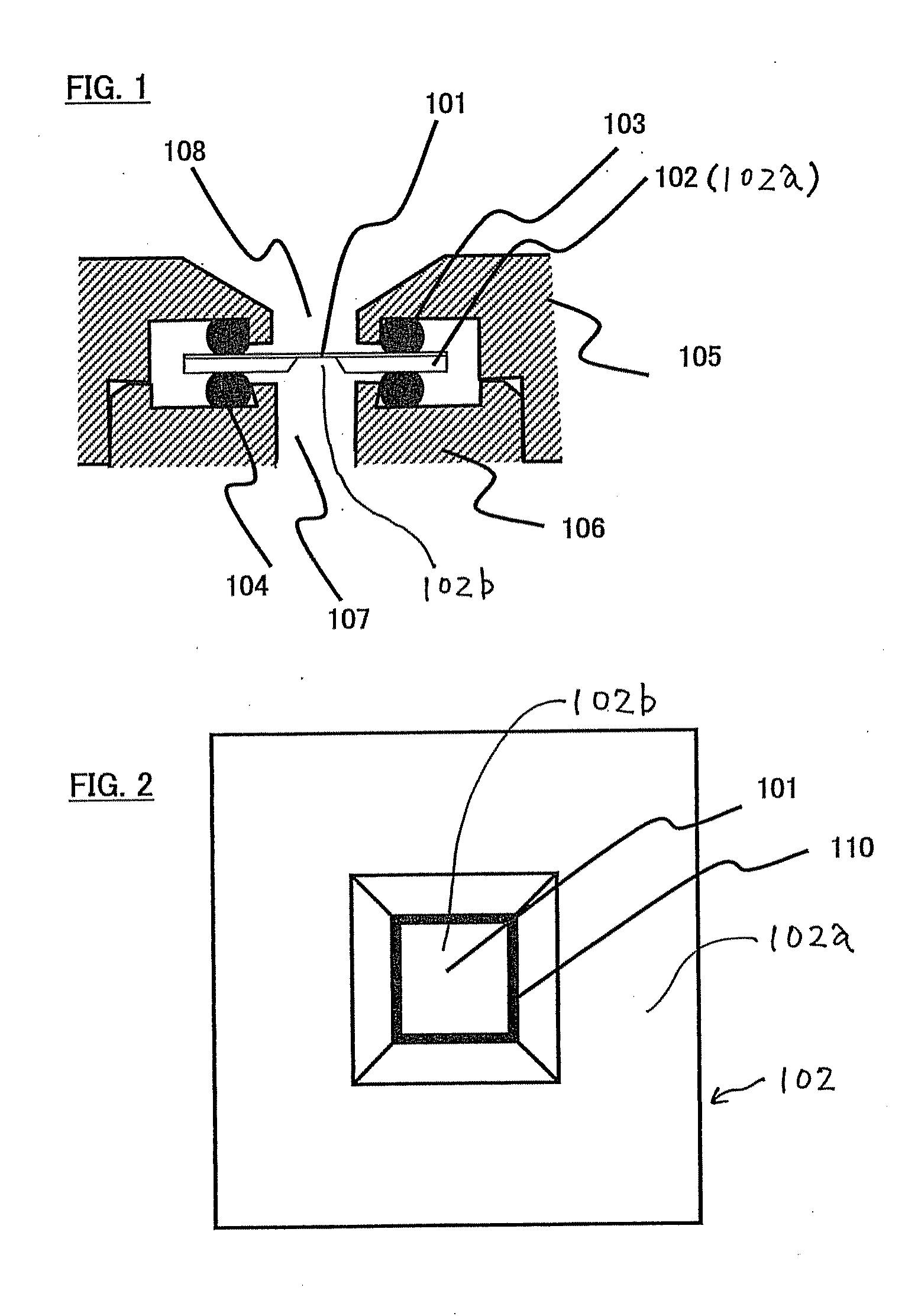
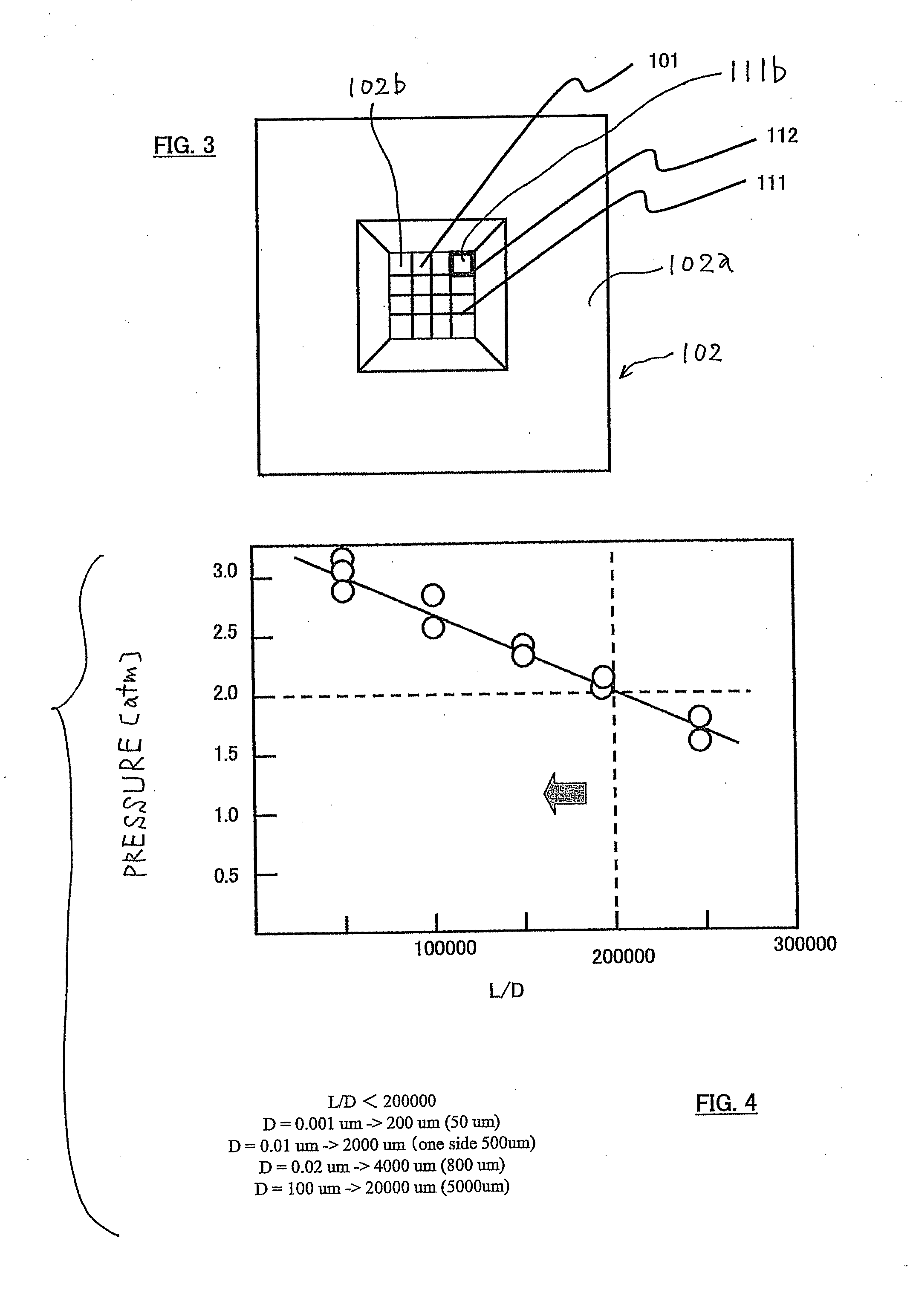
[0068]FIG. 1 shows a sample holder 102 according to the present embodiment and an experimental tool for performing pressure resistance experiments on the sample holder. A sample-holding film 101 is formed on the sample holder 102. A sample (not shown) is placed on a first surface of the film 101. Fundamentally, the sample is placed under atmospheric pressure (atmospheric-pressure ambient).

[0069]On the other hand, a primary beam (electron beam or ion beam) is directed at the sample via the sample-holding film 101 and so the ambient in contact with a second surface of the sample-holding film 101 needs to be pumped down to a vacuum to permit passage of the primary beam while preventing scattering. Therefore, the sample-holding film 101 needs to withstand a differential pressure (i.e., the difference between the pressures of the ambients in contact with the surfaces) of at least 1 atm. In the present invention, it has been determined with some allowance that a resistance withstanding a ...

embodiment 2

[0077]A method of fabricating a sample holder is described by referring to FIG. 5. A silicon substrate 201 is mirror-polished on both its surfaces. Films of silicon nitride 211 and 212 are formed on both surfaces of the substrate using chemical vapor deposition (CVD) (FIG. 5(a)). After lithographically forming a resist pattern 221 using a photoresist, the silicon nitride film 211 is selectively etched using the resist pattern as a mask by RIE (reactive ion etching) (FIG. 5(b)). After removing the resist pattern 221 with sulfuric acid, the silicon substrate 201 is wet-etched using the silicon nitride film 211 as a mask and using KOH solution (FIG. 5(c)). A sample holder having the silicon nitride film 212 can be fabricated by the present sequence of processing steps.

[0078]A method of fabricating a sample holder including a thin film on which a lattice is formed is next described. Both surfaces of an SOI (silicon-on-insulator) wafer 202 (FIG. 6(a)) are mirror-polished. Silicon nitride...

embodiment 3

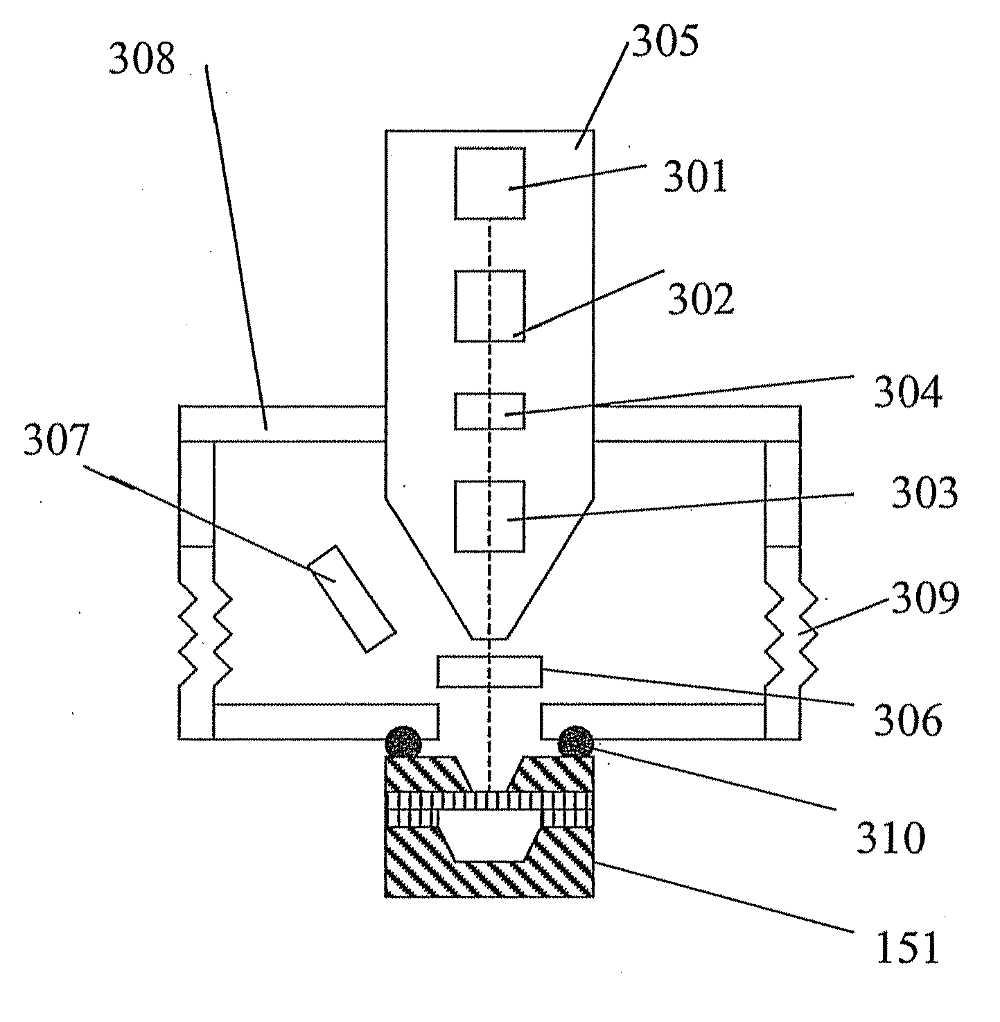
[0084]An observation-and-inspection apparatus, according to one embodiment of the present invention, is schematically shown in FIG. 8. The apparatus includes an electron optics column 305, a backscattered electron detector 306, a secondary electron detector 307, a vacuum chamber 308, a sample driving mechanism 309, and the sample holder 150 described in Embodiment 2. The electron optics column 305 includes an electron source 301, a condenser lens 302, an objective lens 303, and a scanning unit 304. The sample holder 150 is in contact with the vacuum chamber 308 via O-rings 310 and 311 that form support means for supporting the sample holder 150. Therefore, the inside of the chamber 308 can be pumped down to a vacuum or to a reduced-pressure level.

[0085]The sample holder 150 is composed of a frame-like member 150a forming the body of the holder and a sample-holding film 150c in the same way as the foregoing sample holder. The frame-like member 150a is provided with an opening 150b co...


PUM

PropertyMeasurementUnit
thicknessaaaaaaaaaa
thicknessaaaaaaaaaa
thicknessaaaaaaaaaa

Abstract

A sample holder used in SEM (scanning electron microscopy) or TEM (transmission electron microscopy) permitting observation and inspection at higher resolution. The holder has a frame-like member provided with an opening that is covered with a film. The film has a first surface on which a sample is held. The thickness D of the film and the length L of the portion of the film providing a cover over the opening in the frame-like member satisfy a relationship given by L / D <200,000.

Description

BACKGROUND OF THE INVENTION[0001]1. Field of the Invention[0002]The present invention relates to a sample holder permitting a sample to be observed and inspected using an electron beam or ion beam at high resolution in a case where the sample contains moisture or another liquid component. The present invention also relates to a method of observation and inspection using the sample holder. Furthermore, the present invention relates to an observation and inspection apparatus using the sample holder.[0003]2. Description of Related Art[0004]In a sample inspection apparatus having the configuration of a scanning electron microscope (SEM), a sample to be observed or inspected is placed in a sample chamber whose pressure is reduced by vacuum pumping. Under this condition, the sample is irradiated with an electron beam. As a result, secondary signals, such as backscattered electrons and secondary electrons, are emitted from the sample. These secondary signals are detected.[0005]Similarly, i...

Claims


Application Information

Patent Timeline
Patent Type & Authority Applications(United States)
IPC IPC(8): G01N23/02G01N21/01
CPCH01J37/20H01J37/26H01J2237/2004H01J2237/2005H01J2237/28H01J2237/204H01J2237/206H01J2237/262H01J2237/201
Inventor SUGA, MITSUONISHIYAMA, HIDETOSHI
Owner JEOL LTD
Why Eureka
Try Eureka