Single Die MEMS Acoustic Transducer and Manufacturing Method

a manufacturing method and acoustic transducer technology, applied in the field of acoustic microelectricalmechanicalsystem (mems) transducers, can solve the problems of low manufacturing cost, reduced number of separate components, and reduced manufacturing tim

Active Publication Date: 2009-07-02
TDK CORPARATION
View PDF15 Cites 119 Cited by
  • Summary
  • Abstract
  • Description
  • Claims
  • Application Information

AI Technical Summary

Benefits of technology

[0016]The transducer of the present invention also covers embodiments, wherein one or more integrated circuits, such as one or more CMOS circuits, is/are formed in the front surface part of the die, with diaphragm and back plate being electrically connected to the integrated circuit(s) via electrical connections formed in or on the front surface part of the die.
[0017]For embodiments of the transducer of the invention having one or more integrated circuits on the front surface part of the die, then one or more contact pads may be formed in or on the front surface part of the die, said contact pad(s) being electrically connected to the integrated circuit(s) via one or more electrical connections formed in or on the front surface part of the die. It is preferred that at least part of the contact pads are compatible with SMD process techniques and are formed on a substantially plane part of the front surface part of the die.
[0018]However, for other embodiments of the transducer of the invention having one or more integrated circuits on the front surface part of the die, then one or more contact pads may be formed in or on the back surface part of the die, sai

Problems solved by technology

A significant issue in keeping the manufacturing costs low and reliability high for MEMS acoustic transducers is to reduce the number of separate components that need to be manufactured, tested and assembled.
The assembly of multi-component MEMS acoustic transducers has several drawbacks due to the small dimensions of each of these components and the required precise ali

Method used


Image

  • Single Die MEMS Acoustic Transducer and Manufacturing Method
  • Single Die MEMS Acoustic Transducer and Manufacturing Method
  • Single Die MEMS Acoustic Transducer and Manufacturing Method

Examples


first embodiment

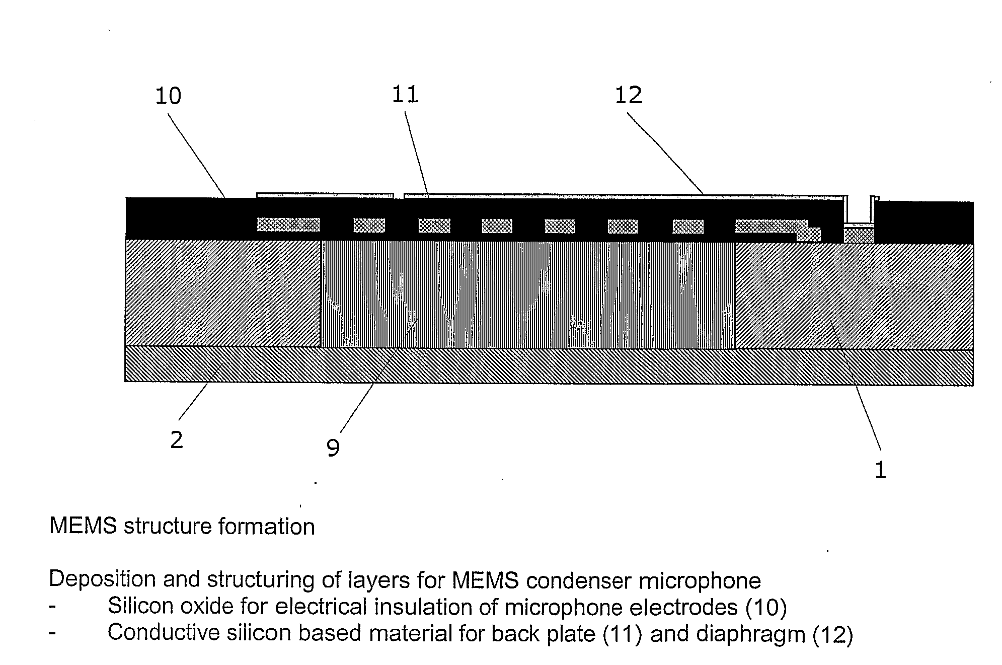
[0109]A silicon microphone manufactured as described above and illustrated in FIGS. 1a-1n, has typically a very low signal output and acts as a signal source with a very high impedance of essentially capacitive nature. In order to obtain a high signal to noise ratio and / or immunity against EMI noise, it is important that the length of the electrical signal paths from the microphone output to the amplifying CMOS circuitry are as short possible with as small parasitic capacitance as practical to minimize signal loss. The present embodiments of the invention provides a solution to this problem by having amplifying circuitry formed on the single die, which also forms the microphone. such a solution is illustrated in FIGS. 2a-2v, which show cross-sectional side views of a semiconductor structure during various steps of manufacturing of a single die condenser microphone with CMOS circuitry formed on the die.

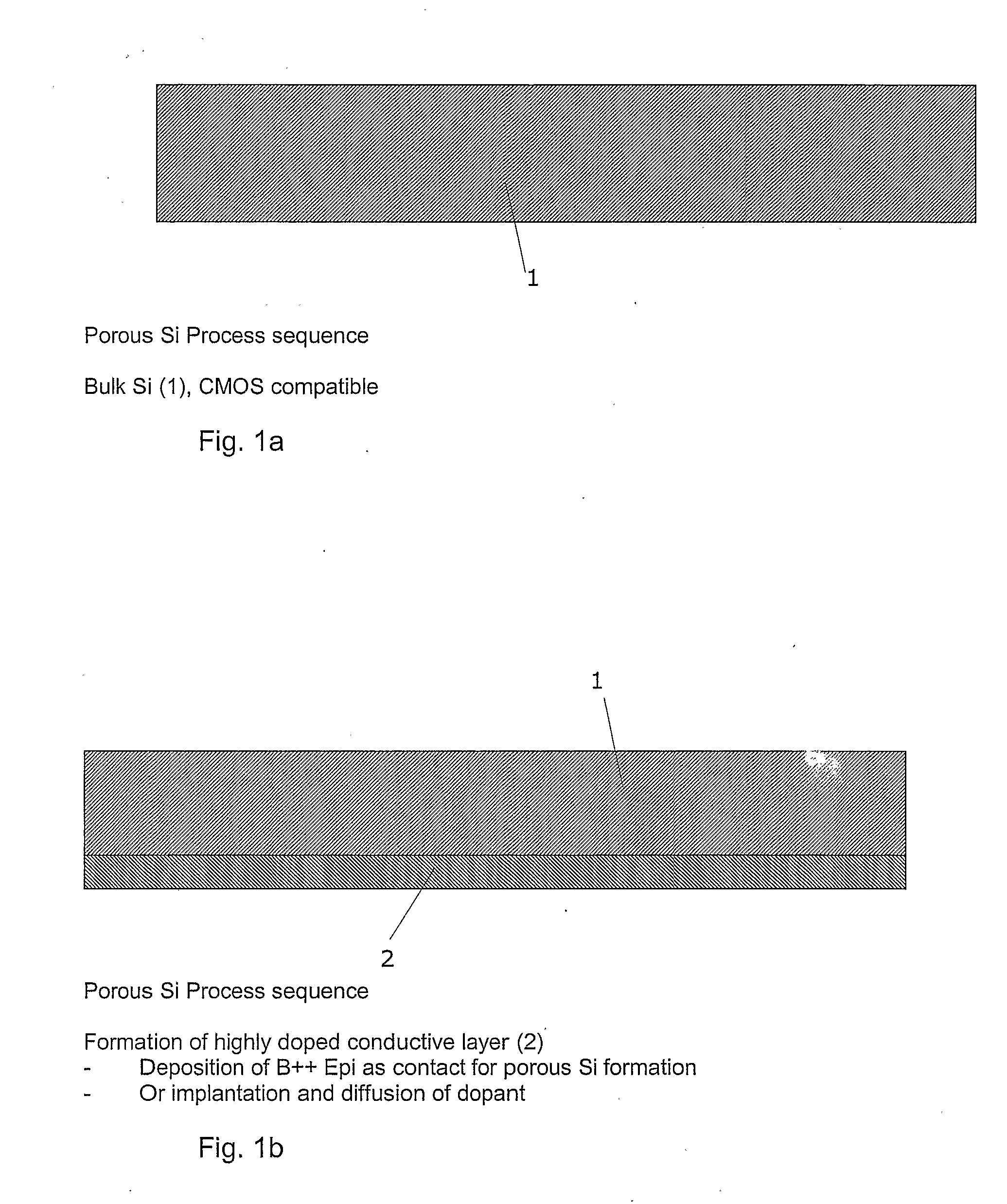
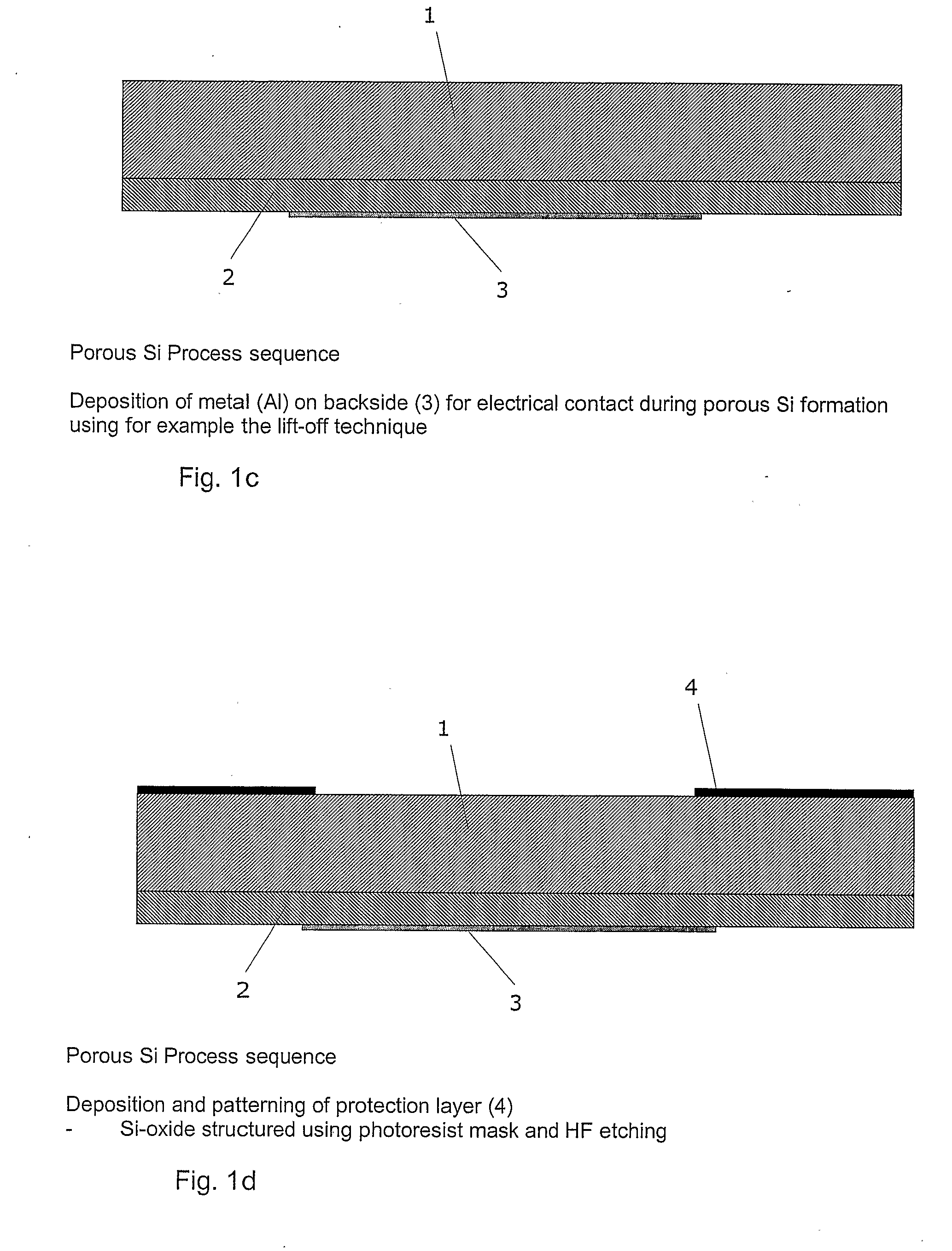
[0110]The steps used in FIGS. 1a-1n are also used for the embodiment illustrated i...

second embodiment

[0144]an acoustic single die MEMS transducer having CMOS circuitry formed on the die is illustrated in FIG. 3.

[0145]The main difference between the single die solutions of FIG. 2v and FIG. 3 is that in FIG. 2v the CMOS circuitry is formed on the front surface part of the die, while for the solution of FIG. 3 the CMOS circuitry is formed on the back surface part of the die. The process steps used to produce the single die MEMS transducer of FIG. 3 are similar to the process steps of FIGS. 2a-2v, but the CMOS integration is performed on the backside of the wafer in stead of on the front side of the wafer as illustrated in FIG. 2f. Here the CMOS has to be processed into regions of the backside of the die that did not receive the high doping so that a CMOS compatible die surface is maintained. For that purpose the doping has to be performed selectively for example by ion implantation through an oxide or photoresist mask.

[0146]It is also noted that for single die MEMS transducer illustra...

third embodiment

[0148]an acoustic single die MEMS transducer having CMOS circuitry formed on the die is illustrated in FIG. 4.

[0149]The main difference between the single die solutions of FIG. 2v and FIG. 4 is that in FIG. 4 there are no contact pads on the backside of the die, and hence there are no feedthroughs for obtaining electrical contact from the front to the backside of the die. Thus the steps illustrated in FIGS. 2c-2e are omitted for the solution of FIG. 4, and the backside contact steps illustrated in FIGS. 2n-2p are replaced by corresponding steps for providing front side contacts, to thereby obtain electrical contact to the CMOS circuitry on the front side. Also for the single die MEMS transducer illustrated in FIG. 4, there is no backside Si-oxide layer between the backside of the silicon substrate and the sealing capping layer, see the above discussion given in connection with FIG. 3.

[0150]For the embodiment of FIG. 4, the front side contacts have SMD bump pads, which are reaching h...


PUM


Abstract

The invention relates to an acoustic micro-electrical-mechanical-system (MEMS) transducer formed on a single die based on a semiconductor material and having front and back surface parts opposed to each other. The invention further relates to a method of manufacturing such an acoustic MEMS transducer. The acoustic MEMS transducer comprises a cavity formed in the die to thereby provide a back volume with an upper portion facing an opening of the cavity and a lower portion facing a bottom of the cavity. A back plate and a diaphragm are arranged substantially parallel with an air gap there between and extending at least partly across the opening of the cavity, with the back plate and diaphragm being integrally formed with the front surface part of the die. The bottom of the cavity is bounded by the die. The diaphragm may be arranged above the back plate and at least partly extending across the back plate. It is preferred that the backside openings are formed in the die with the openings extending from the back surface part of the die to the cavity bottom. Part of or all of the backside openings may be acoustically sealed by a sealing material.

Description

FIELD OF THE INVENTION[0001]The present invention relates to an acoustic micro-electrical-mechanical-system (MEMS) transducer formed on a single die based on a semiconductor material.BACKGROUND OF THE INVENTION[0002]MEMS acoustic transducers for application in portable communication devices such as mobile terminals and hearing prostheses must be robust devices of small size and low cost and still maintain good electro-acoustic performance, reliability and operability. A significant issue in keeping the manufacturing costs low and reliability high for MEMS acoustic transducers is to reduce the number of separate components that need to be manufactured, tested and assembled. The assembly of multi-component MEMS acoustic transducers has several drawbacks due to the small dimensions of each of these components and the required precise alignment of each of these components. The delicate assembly process increases manufacturing time and leads to yield loss, which translates to increased m...

Claims


Application Information

Patent Timeline
IPC IPC(8): H04R25/00H01L21/302
CPCH04R31/00H04R19/005H04R19/04
Inventor ROMBACH, PIRMINARNOLDUS, MORTEN BERGGINNERUP, MORTEN
Owner TDK CORPARATION
Why Eureka
Try Eureka