Nonvolatile memory and three-state FETs using cladded quantum dot gate structure

a quantum dot gate structure, non-volatile memory technology, applied in transistors, solid-state devices, instruments, etc., can solve the problems of small control over the location of si nanoparticles in the gate, the size of the gate, and the separation between, and the problem of dot size variation inherent in conventional fabrication techniques

Active Publication Date: 2009-07-09
JAIN FAQUIR C
View PDF12 Cites 57 Cited by
  • Summary
  • Abstract
  • Description
  • Claims
  • Application Information

AI Technical Summary

Problems solved by technology

In the current quantum dot gate device processing there is little control over the location of Si nanoparticles in the gate, their sizes, as well as the separation between them.
Here, they again suffer from the dot size variation problem inherent in conventional fabrication techniques including those employ self-organization.

Method used


Image

  • Nonvolatile memory and three-state FETs using cladded quantum dot gate structure
  • Nonvolatile memory and three-state FETs using cladded quantum dot gate structure
  • Nonvolatile memory and three-state FETs using cladded quantum dot gate structure

Examples


Embodiment Construction

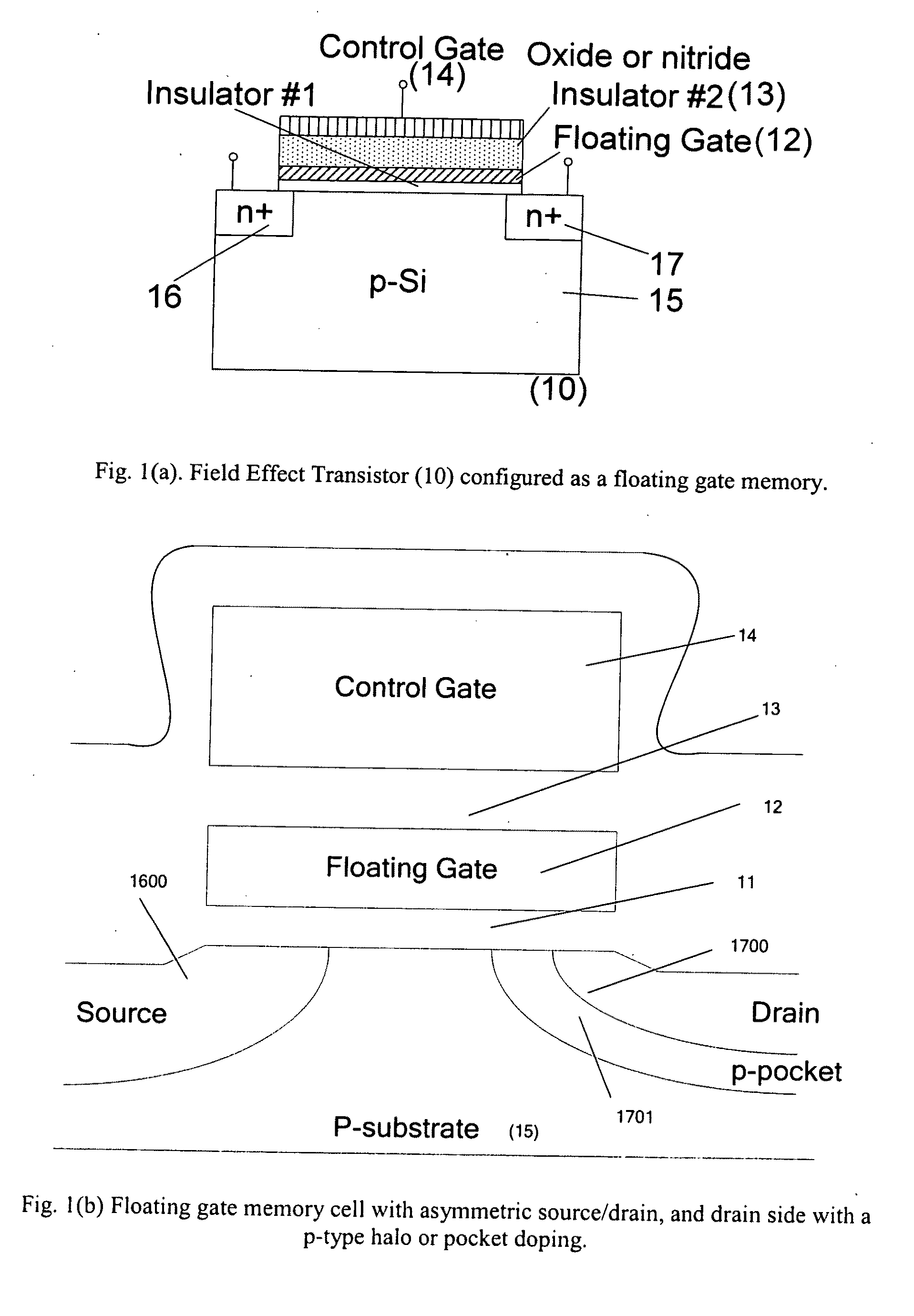
[0034]FIG. 1(a). shows Cross-sectional schematic of a conventional floating gate nonvolatile memory. Here the Si field-effect transistor (FET) has two gates. The first gate is the floating gate (12), which is deposited on a thin insulator layer (11), and holding the desired charge determining the state of the memory [0 or 1], and the second gate (14) serves as the control gate which is separated by an insulator layer (13) for the memory. The source (16) and drain (17) regions are shown as n+ regions in p-Si substrate (15). The control gate could be simple metal layer (14) or appropriately doped poly-Si layer (not shown here) with the metal contact layer.

[0035]FIG. 1(b) shows floating gate memory with asymmetric source (1600) and drain (1700) regions. The drain side is shown with a p-pocket or p-type halo doping (1701) to tailor the drain characteristics of the FET.

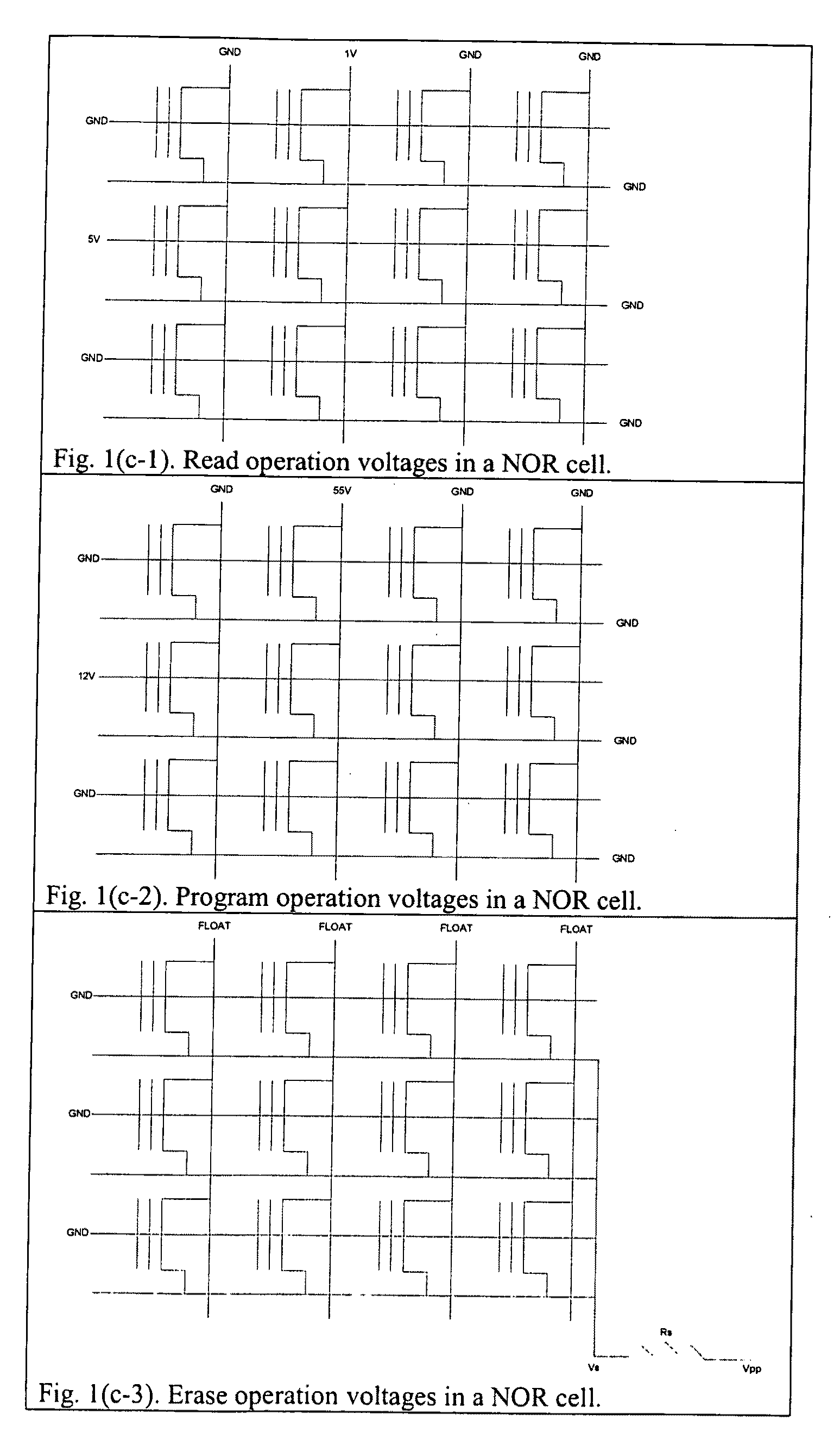
[0036]FIG. 1(c-1 to c-3). NOR cell architecture showing ‘Read’ in FIG. 1c-1; Write in FIG. 1c-2; and ‘Erase’ in FIG. 1c-...


PUM


Abstract

The present invention discloses use of quantum dot gate FETs as a nonvolatile memory element that can be used in flash memory architecture as well as in a nonvolatile random access memory (NVRAM) configuration that does not require refreshing of data as in dynamic random access memories. Another innovation is the design of quantum dot gate nonvolatile memory and 3-state devices using modulation doped field-effect transistors (MODFETs), particularly MOS-gate field effect transistors. The cladded quantum dot gate MODFETs can be designed in Si—SiGe, InGaAs—InP and other material systems. The incorporation of 3-state FET devices in static random access memory (SRAM) cell is described to result in advanced multi-state memory operation. Unlike conventional SRAMs, the 3-state QD-FET based of SRAMs provides 3 and 4-state memory operation due to the utilization of the intermediate states particularly in CMOS configuration. QD-gate FETs, potentially suitable for 8 nm channel lengths, in vertical configuration (VFET) are also described.

Description

[0001]This application is a Continuation-in-part of application Ser. No. 12 / 006974, filed Jan. 9, 2008 (pending)BACKGROUND OF THE INVENTION[0002]1. Field of the Invention[0003]This invention relates to field-effect transistors (FETs), MOS (Metal Oxide Semiconductor) devices, and MOS-gate modulation doped field-effect transistors (MODFETs) in which the gate consists of a layer or layer(s) of cladded nanoparticles or cladded quantum dots. The device structure behaves as fast access nonvolatile memory structure or as a FET exhibiting multiple states (such as three-state) in its drain current-gate voltage characteristics depending on the configuration of the layers in the gate region which consists layers of cladded quantum dots and thin insulating films. In particular, MOS gate quantum dot nonvolatile memory and 3-state devices in MODFET structural configuration are described. MODFET configured as self-aligned MOS gate incorporating QD layers in gate and asymmetric couple well transpor...

Claims


Application Information

Patent Timeline
Patent Type & Authority Applications(United States)
IPC IPC(8): H01L29/06
CPCG11C11/412G11C11/56H01L21/28273H01L21/28282H01L27/1104H01L27/11521H01L29/7783H01L29/42332H01L29/42348H01L29/66825H01L29/66833H01L29/7782H01L29/1054H01L29/40114H01L29/40117H10B10/12H10B41/30
Inventor JAIN, FAQUIR C.
Owner JAIN FAQUIR C
Why Eureka
Try Eureka