Thin film transistor, display device including the same, and method for manufacturing the same

a technology display devices, applied in semiconductor devices, instruments, computing, etc., can solve the problems of complex manufacturing process, increased cost and time required, and difficulty in simultaneously satisfying the characteristics of thin film transistors having the same structure, etc., to achieve improved crystallinity, increase charge mobility, and increase the effect of effective energy density

Active Publication Date: 2009-07-09
SHENZHEN CHINA STAR OPTOELECTRONICS TECH CO LTD
View PDF1 Cites 8 Cited by
  • Summary
  • Abstract
  • Description
  • Claims
  • Application Information

AI Technical Summary

Benefits of technology

[0035]Also, when crystallizing the semiconductor using the laser, a crack of the semiconductor is not generated at a step portion of the circuit control electrode, and the crystallization may be uniformly executed. Also, the effective energy density is increased and the crystallinity is improved, thereby increasing the charge mobility.
[0036]Also, it is not necessary for the thickness of the control electrode to be reduced such that as addition process is not necessary and a sufficient process margin may be obtained, and it is not necessary for the thickness of the gate insulating layer to be thicker such that the mobility current may be increased and sufficient storage capacitance may be gained.

Problems solved by technology

However, these characteristics are trade offs with respect to one another such that it is difficult for thin film transistors having the same structure to simultaneously satisfy these characteristics.
However, the manufacturing process is complicated and the cost and time required are remarkably increased for various thin film transistors having different characteristics in one display panel.

Method used


Image

  • Thin film transistor, display device including the same, and method for manufacturing the same
  • Thin film transistor, display device including the same, and method for manufacturing the same
  • Thin film transistor, display device including the same, and method for manufacturing the same

Examples


exemplary embodiment 1

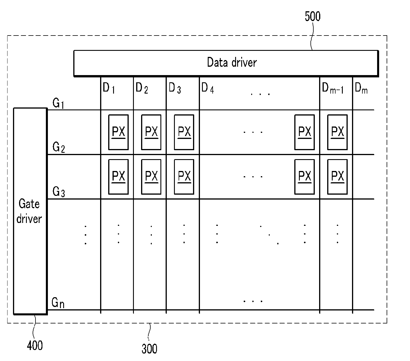
[0051]First, a display device according to an exemplary embodiment of the present invention will be described with the reference to FIG. 1.

[0052]FIG. 1 is a schematic diagram of a display device according to an exemplary embodiment of the present invention.

[0053]Referring to FIG. 1, a display device according to an exemplary embodiment of the present invention includes a display panel unit 300 made of one or two display panels.

[0054]The display panel unit 300 includes a plurality of pixels, a plurality of gate lines G1-Gn, a plurality of data lines D1-Dm, a gate driver 400 and a data driver 500.

[0055]The gate lines G1-Gn transmit gate signals, and the data lines D1-Dm transmit data signals and cross the gate lines G1-Gn.

[0056]The pixels PX are connected to the gate lines G1-Gn, and the data lines D1-Dm, and are arranged substantially in a matrix. Each pixel PX includes a switching element (not shown) such as a thin film transistor.

[0057]The gate driver 400 is connected to the gate l...

exemplary embodiment 2

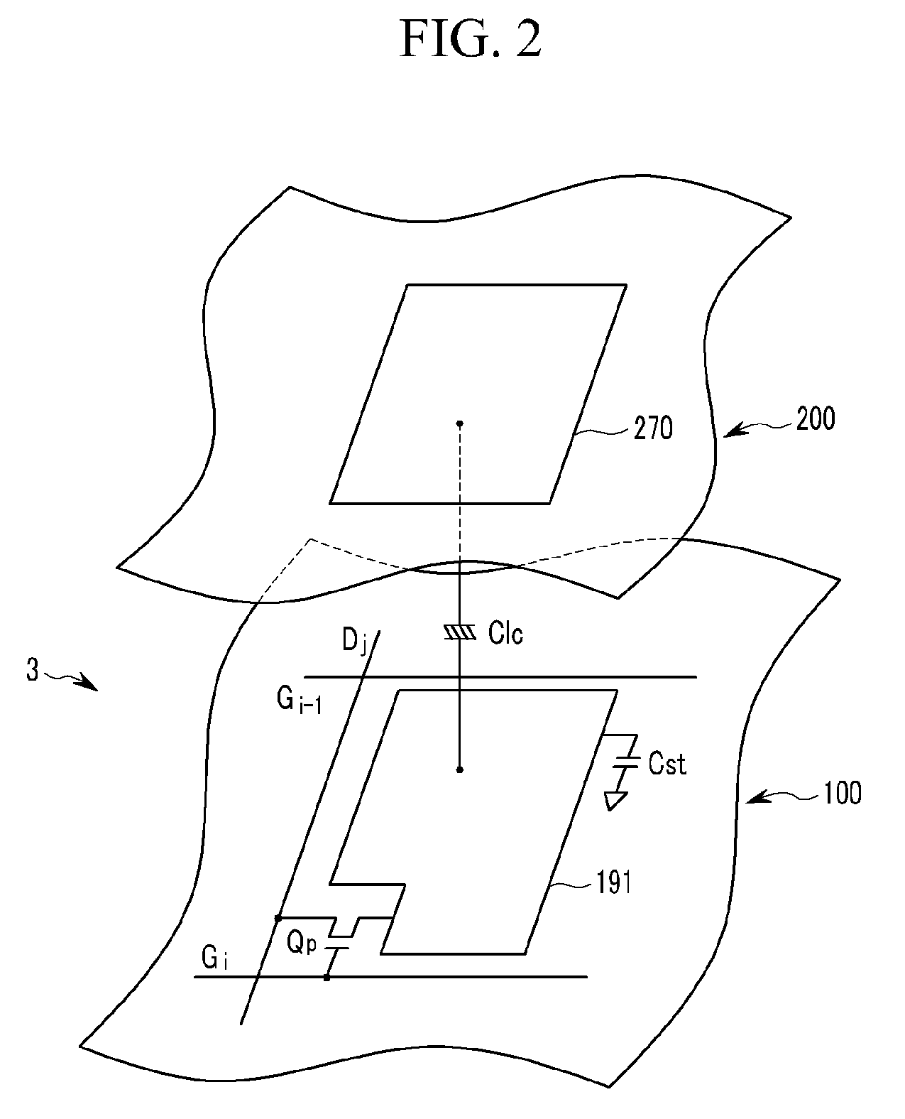
[0118]Next, another exemplary embodiment of the present invention will be described with reference to FIGS. 13 to 15. The present exemplary embodiment relates to an active matrix OLED display. Descriptions overlapping the previous exemplary embodiment are omitted, and the same constituent elements are indicated by the same reference numerals.

[0119]FIG. 13 is an equivalent circuit schematic diagram of an OLED display according to an exemplary embodiment of the present invention.

[0120]Referring to FIG. 13, an OLED display according to the present exemplary embodiment includes a plurality of signal lines 121, 171 and 172, and a plurality of pixels PX connected thereto and substantially arranged in a matrix.

[0121]The signal lines include a plurality of gate signal lines 121 for transmitting gate signals (or scanning signals), a plurality of data signal lines 171 for transmitting data signals and a plurality of driving voltage lines 172 for transmitting a driving voltage. The gate signal...


PUM


Abstract

A display device and a manufacturing method thereof, include a first thin film transistor including a first control electrode, a first semiconductor disposed on the first control electrode, and a first input electrode and a first output electrode opposite to each other on the first semiconductor; and a second thin film transistor including a second control electrode, a second semiconductor disposed on the second control electrode, and a second input electrode and a second output electrode opposite to each other on the second semiconductor, wherein the first semiconductor includes a first lower semiconductor including polysilicon, and a first upper semiconductor disposed on the first lower semiconductor, the first upper semiconductor including amorphous silicon.

Description

[0001]This application claims priority to Korean Patent Application No. 10-2008-0001369, filed on Jan. 4, 2008, and all the benefits accruing therefrom under 35 U.S.C. §119, the contents of which in their entirety are herein incorporated by reference.BACKGROUND OF THE INVENTION[0002](a) Field of the Invention[0003]The present invention relates to a thin film transistor, a display device including the same and a manufacturing method thereof.[0004](b) Description of the Related Art[0005]A display device such as a liquid crystal display (“LCD”), an organic light emitting diode (“OLED”) display and an electrophoretic display includes a plurality of pixels. Each pixel includes a pair of field generating electrodes and an optical active layer formed therebetween. For example, the LCD includes a liquid crystal capacitor having a liquid crystal layer as the optical active layer between the field generating electrodes, and the OLED display includes an organic light emitting element having an...

Claims


Application Information

Patent Timeline
Patent Type & Authority Applications(United States)
IPC IPC(8): G06F3/038
CPCG09G3/3233G09G2300/0439G09G2300/0842H01L27/1229H01L27/1251H01L29/78696H01L27/3262H01L29/66765H01L29/78669H01L29/78678H01L27/1288H10K59/1213H01L27/1222
Inventor SONG, JUN-HOKIM, JOO-HANKIM, HYUNG-JUNCHO, SUNG-HAENGJEONG, KI-HUNSHIM, SEUNG-HWAN
Owner SHENZHEN CHINA STAR OPTOELECTRONICS TECH CO LTD
Why Eureka
Try Eureka