Metal gate stack and semiconductor gate stack for CMOS devices

a metal gate stack and semiconductor technology, applied in the field of semiconductor gate stacks, can solve the problems of illusive, high-k material metal gate stacks for p-type field effect transistors that are capable, and the identification of materials for a dual work function metal gate electrode system has presented some challenges

Inactive Publication Date: 2009-07-16
TAIWAN SEMICON MFG CO LTD
View PDF16 Cites 62 Cited by
  • Summary
  • Abstract
  • Description
  • Claims
  • Application Information

AI Technical Summary

Benefits of technology

[0006]The present invention addresses the needs described above by providing a CMOS structure including a diffusion barrier layer directly on the sidewalls

Problems solved by technology

So far, identification of materials for a dual work function metal gate electrode system has presented some challenges.
In particular, a high-k material metal gate stack for p-type field effect transistors that is capable of withstanding a high temperature thermal cycling encountered during a conventional semiconductor processing sequence has proven to be illusive so far.
However, integration of th

Method used


Image

  • Metal gate stack and semiconductor gate stack for CMOS devices
  • Metal gate stack and semiconductor gate stack for CMOS devices
  • Metal gate stack and semiconductor gate stack for CMOS devices

Examples


Embodiment Construction

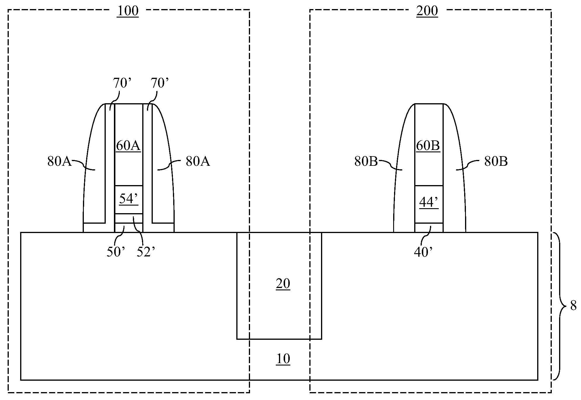
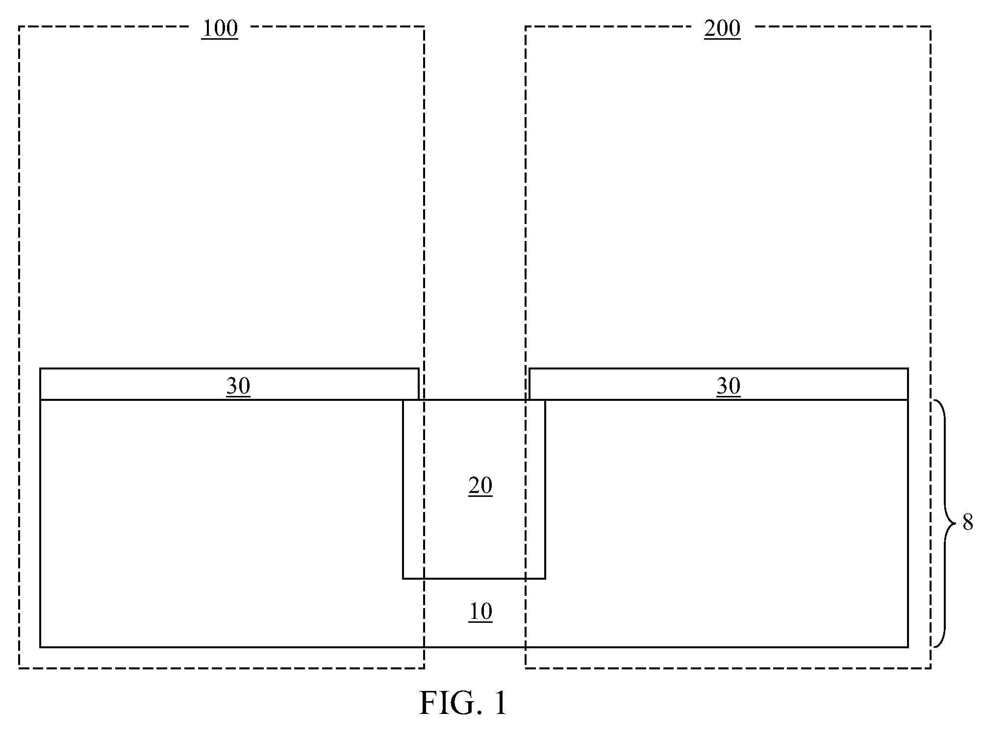
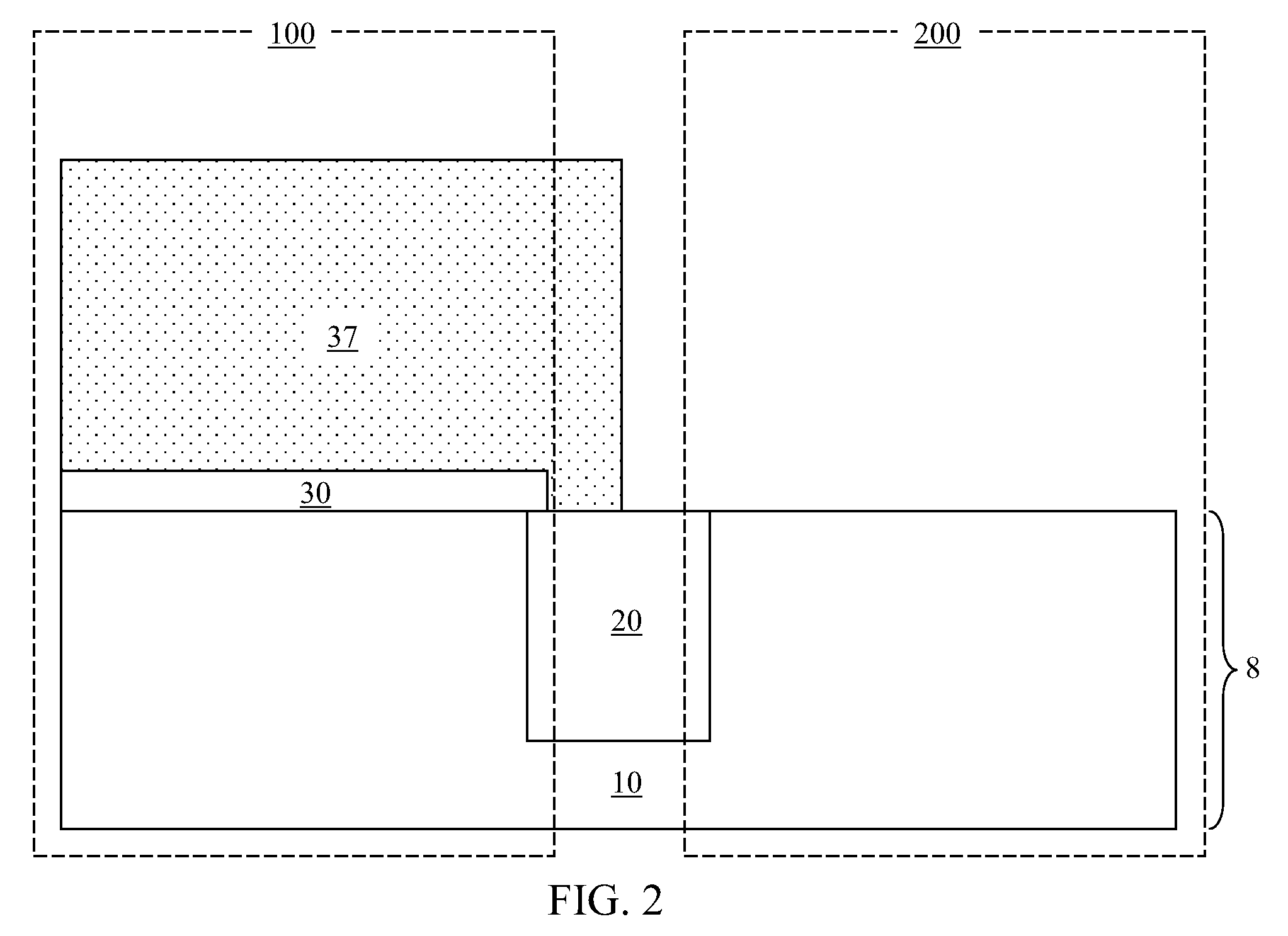
[0040]As stated above, the present invention relates to complementary metal-oxide-semiconductor (CMOS) devices having a metal gate stack transistor and a semiconductor gate stack transistor, and methods of manufacturing the same, which are now described in detail with accompanying figures. It is noted that like and corresponding elements are referred to by like reference numerals.

[0041]Referring to FIG. 1, an exemplary semiconductor structure according to the present invention is shown, which comprises a semiconductor substrate 8 containing a substrate semiconductor layer 10 and a shallow trench isolation structure 20. The substrate semiconductor layer 10 comprises a semiconductor material, which may be selected from, but is not limited to, silicon, germanium, silicon-germanium alloy, silicon carbon alloy, silicon-germanium-carbon alloy, gallium arsenide, indium arsenide, indium phosphide, III-V compound semiconductor materials, II-VI compound semiconductor materials, organic semico...


PUM


Abstract

A semiconductor gate stack comprising a silicon oxide based gate dielectric and a doped semiconductor material is formed on a semiconductor substrate. A high-k material metal gate electrode comprising a high-k gate dielectric and a metal gate portion is also formed on the semiconductor substrate. Oxygen-impermeable dielectric spacers are formed on the sidewalls of the semiconductor gate stack and the high-k material metal gate stack. The oxygen-impermeable dielectric spacer on the semiconductor gate stack is removed, while the oxygen impermeable dielectric spacer on the high-k material metal gate electrode is preserved. A low-k dielectric spacer is formed on the semiconductor gate stack, which provides a low parasitic capacitance for the device employing the semiconductor gate stack.

Description

FIELD OF THE INVENTION[0001]The present invention generally relates to semiconductor devices, and particularly to complementary metal-oxide-semiconductor (CMOS) devices having a metal gate stack transistor and a semiconductor gate stack transistor, and methods of manufacturing the same.BACKGROUND OF THE INVENTION[0002]Complementary metal oxide semiconductor (CMOS) integration requires two gate materials, one having a work function near the valence band edge of the semiconductor material in the channel and the other having a work function near the conduction band edge of the same semiconductor material. In CMOS devices having a silicon channel, a conductive material having a work function of about 4.0 eV is necessary for n-type metal oxide semiconductor field effect transistors (NMOSFETs) and another conductive material having a work function of about 5.0 eV is necessary for p-type metal oxide semiconductor field effect transistors (PMOSFETs).[0003]In conventional CMOS devices employ...

Claims


Application Information

Patent Timeline
IPC IPC(8): H01L29/78H01L21/336
CPCH01L21/82345H01L21/823462H01L21/823468H01L21/823842H01L21/823857H01L21/823864H01L29/78H01L29/4966H01L29/4983H01L29/517H01L29/518H01L29/6656H01L27/092
Inventor ADAMS, CHARLOTTE D.DORIS, BRUCE B.FISHER, PHILIPHENSON, WILLIAM K.SLEIGHT, JEFFREY W.
Owner TAIWAN SEMICON MFG CO LTD
Why Eureka
Try Eureka