Method for manufacturing ferroelectric memory

a manufacturing method and technology for ferroelectric memories, applied in the direction of niobium compounds, fixed capacitors, coatings, etc., can solve the problems of difficult adjustment of composition ratio, deterioration of ferroelectric fatigue characteristics, and failure to obtain ferroelectric films with desired ferroelectric characteristics, so as to prevent the difference in ferroelectric characteristics of ferroelectric films and excellent ferroelectric characteristics

Inactive Publication Date: 2009-07-23
SEIKO EPSON CORP
View PDF8 Cites 4 Cited by
  • Summary
  • Abstract
  • Description
  • Claims
  • Application Information

AI Technical Summary

Benefits of technology

[0012]In accordance with an advantage of some aspects of the invention, there is provided a method for manufacturing a ferroelectric memory device, by which differences in the ferroelectric characteristics of ferroelectric films can be prevented from occurring, and excellent ferroelectric characteristics can be obtained.

Problems solved by technology

However, when ferroelectric films are formed by a solution method, the following two problems arise, particularly in connection with the solution containing ferroelectric materials to be used.
When Pb is below this range, deterioration in the fatigue characteristic of ferroelectric films occurs.
In contrast, according to the solution method, the Pb composition ratio is decided by the metal composition within the material solution that has been prepared, such that it is very difficult to adjust the composition ratio within the optimum range by film formation by coating, such as, spin coat method to be conducted later.
When the chemical reactions in the solution state progress above a certain level, a ferroelectric film having desired ferroelectric characteristics may not be obtained even when the film forming process and heating process are conducted by using the material solution.
However, the serviceable life of PZT type material solution may often be short, for example, for about a week to a month.

Method used


Image

  • Method for manufacturing ferroelectric memory
  • Method for manufacturing ferroelectric memory
  • Method for manufacturing ferroelectric memory

Examples


Embodiment Construction

[0025]Preferred embodiments of the invention are described below in detail with reference to the accompanying drawings.

[0026]Method for Manufacturing Ferroelectric Film

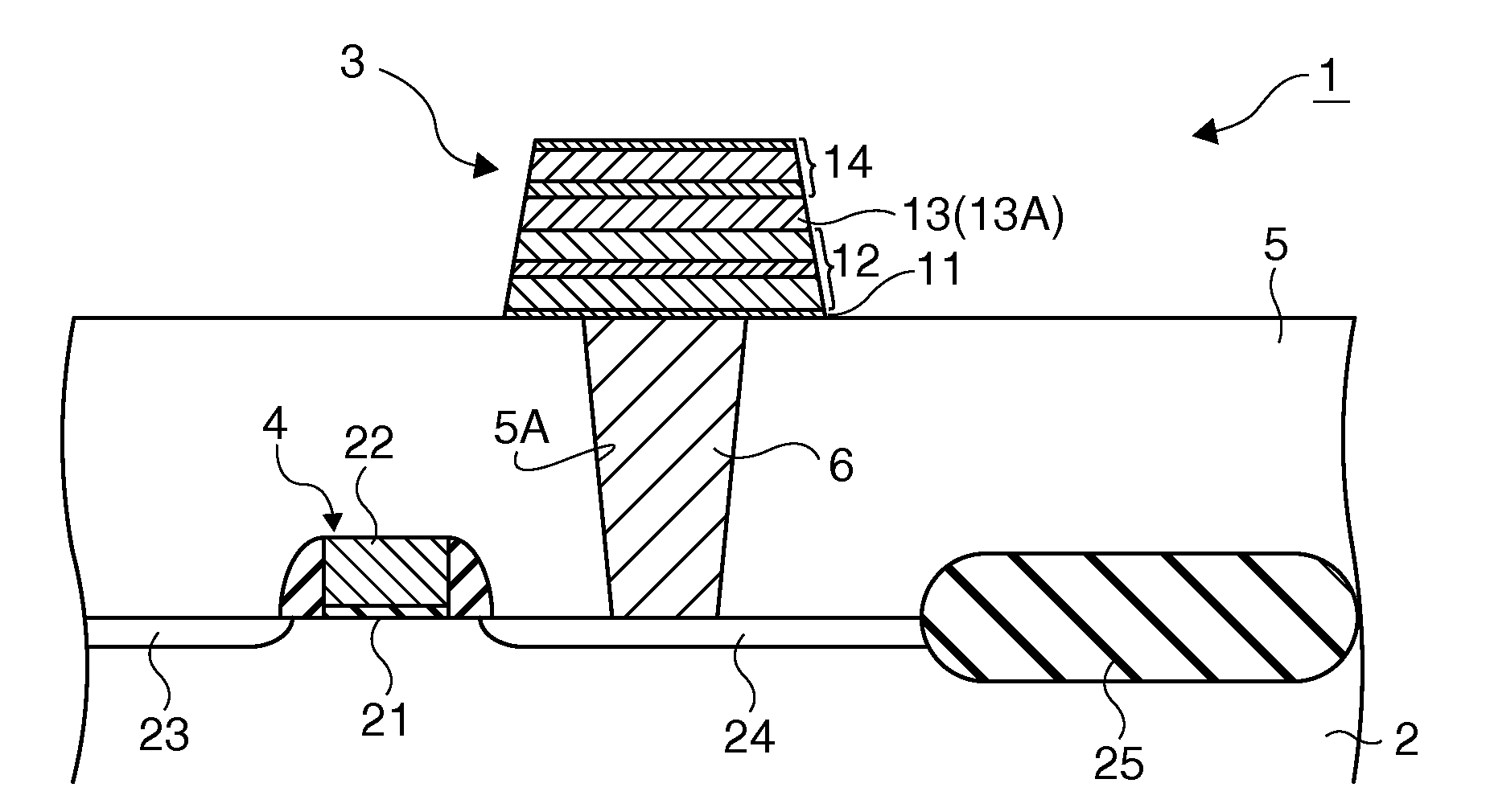
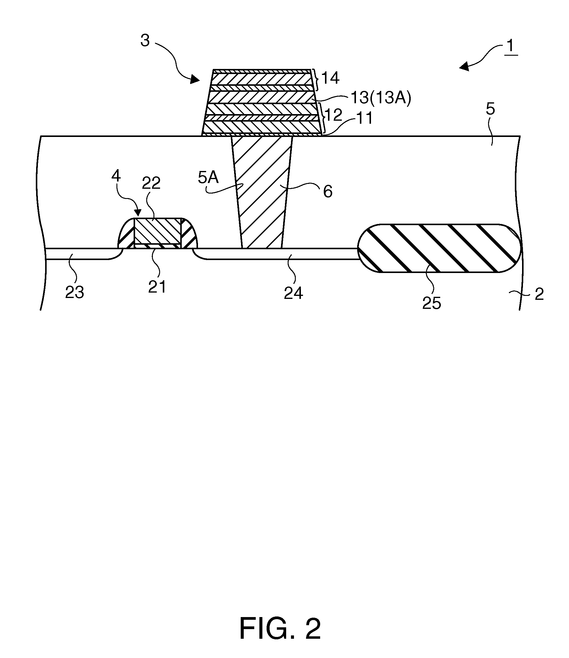
[0027]In accordance with an embodiment of the invention, a ferroelectric film composed of compound having perovskite type crystal structure expressed by ABO3 type is manufactured. As a concrete example, the embodiment is described as to the case where the ferroelectric film is composed of compound having perovskite type crystal structure expressed by Pb (Zr, Ti, Nb) O3 (hereafter referred to as PZTN).

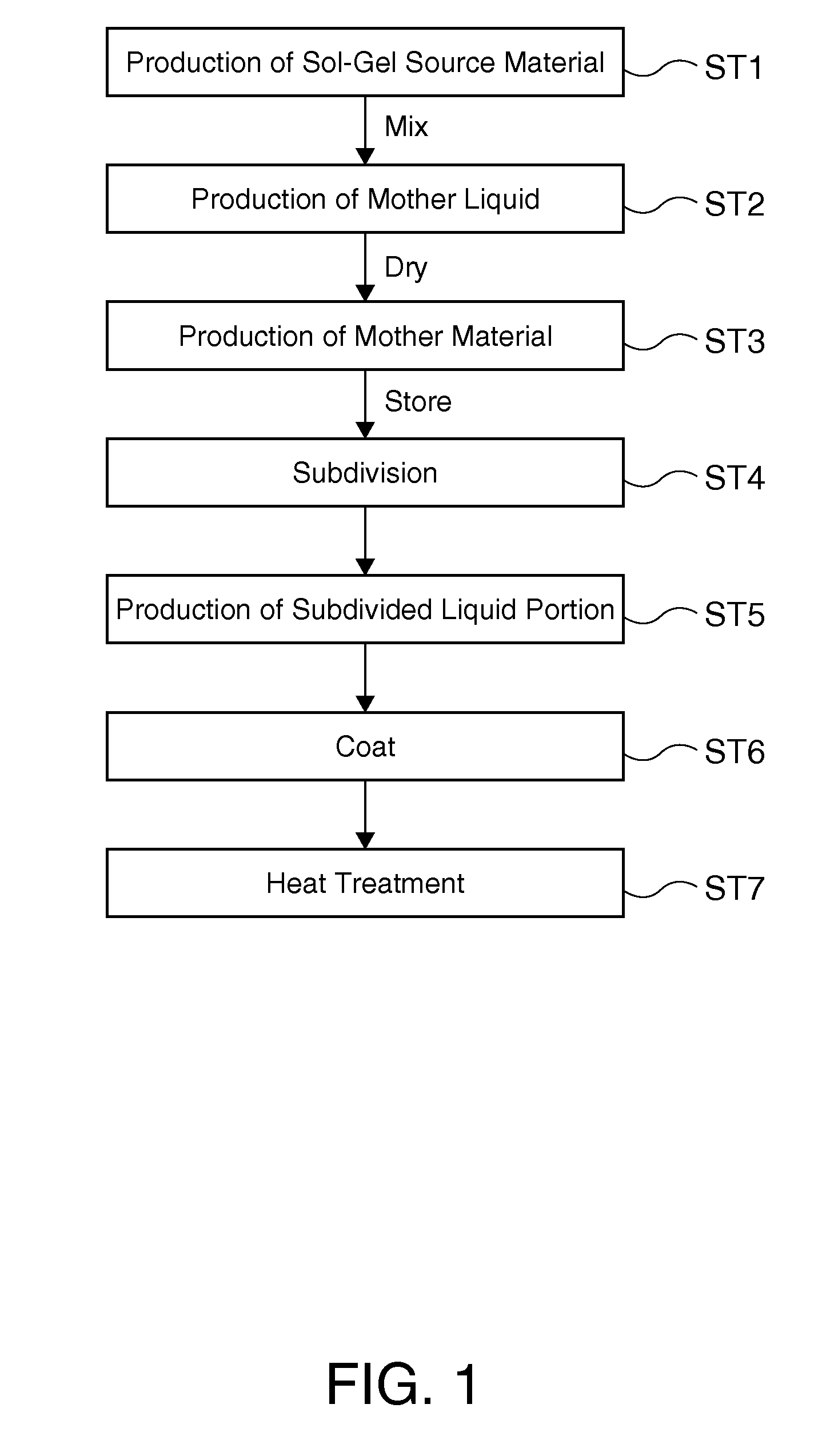
[0028]A method for manufacturing a ferroelectric film composed of PZTN is described with reference to a flowchart in FIG. 1. First, a first sol-gel source material solution containing Pb as A site metal and Zr as B site metal in the compound is prepared. Similarly, a second sol-gel source material solution containing Pb as A site metal and Ti as B site metal in the compound is prepared, and a third sol-gel source material...


PUM

PropertyMeasurementUnit
timeaaaaaaaaaa
timeaaaaaaaaaa
boiling pointaaaaaaaaaa

Abstract

A method for manufacturing a ferroelectric memory includes the steps of: preparing a sol-gel solution; removing solvent from the sol-gel solution to obtain powder; dividing the powder into at least first powder and second powder; obtaining solution with the first powder; coating the solution on a first conductive film; and applying heat treatment to the solution on the first conductive film to form a ferroelectric film.

Description

[0001]The entire disclosure of Japanese Patent Application No. 2008-007851, filed Jan. 17, 2008 is expressly incorporated by reference herein.BACKGROUND[0002]1. Technical Field[0003]The present invention relates to methods for manufacturing ferroelectric memories.[0004]2. Related Art[0005]Ferroelectric memory devices (FeRAM) are nonvolatile memory devices capable of low voltage and high-speed operation, using spontaneous polarization of the ferroelectric material, and their memory cells can be each formed from one transistor and one capacitor (1T / 1C). Accordingly, ferroelectric memory devices can achieve integration at the same level of that of DRAM, and are therefore expected as large-capacity nonvolatile memories.[0006]As the material for forming ferroelectric films that compose ferroelectric capacitors, in other words, as the ferroelectric material, a material composed of compound having a perovskite type crystal structure expressed as an ABO3 type may preferably be used. Above a...

Claims


Application Information

Patent Timeline
Patent Type & Authority Applications(United States)
IPC IPC(8): B05D5/12
CPCC01G33/006C01P2002/34C01P2006/40H01L28/56H01L21/31691H01L27/11502H01G4/1245H01L21/02282H01L21/02197H10B53/00H01L21/02356
Inventor KUROKAWA, KENICHITAMURA, HIROAKINAWANO, MASAHISA
Owner SEIKO EPSON CORP
Why Eureka
Try Eureka