Component of substrate processing apparatus and method for forming a film thereon

Active Publication Date: 2009-07-23
TOKYO ELECTRON LTD
View PDF4 Cites 3 Cited by
  • Summary
  • Abstract
  • Description
  • Claims
  • Application Information

AI Technical Summary

Benefits of technology

[0024]If the base is connected to the anode of a power supply and immersed in a solution mainly formed of an organic acid, an oxide film grows inward from the surface of the substrate, whereas the amount of an oxide film growing outward from the surface of the substrate is small. That is, since the amount of oxide crystal columns growing outward from the surface is small, the development of compressive stress by the collision between the crystal columns can be greatly suppressed.
[0025]Further, the crystal columns of oxide grow radially from the silicon of the base as a nucleus, and thus the crystal structure of the film is not al

Problems solved by technology

In recent years, the substrate processing apparatus has increased in size with the increase in the diameter of wafer and, therefore, the increase in the weight of the substrate processing apparatus has become an issue to be concerned about.
In the high power plasma processing, the temperature of a cooling plate rises, but a sealed alumite film generally has a low heat resistance.
For this reason, in the plasma processing, damages such as cracks develop in the alumite film formed on the

Method used


Image

  • Component of substrate processing apparatus and method for forming a film thereon
  • Component of substrate processing apparatus and method for forming a film thereon
  • Component of substrate processing apparatus and method for forming a film thereon

Examples


Embodiment Construction

[0032]Hereinafter, an embodiment of the present invention will be described with reference to the accompanying drawings which form a part hereof.

[0033]First, a description will be made on a substrate processing apparatus to which a component of a substrate processing apparatus in accordance with the embodiment of the present invention is applied.

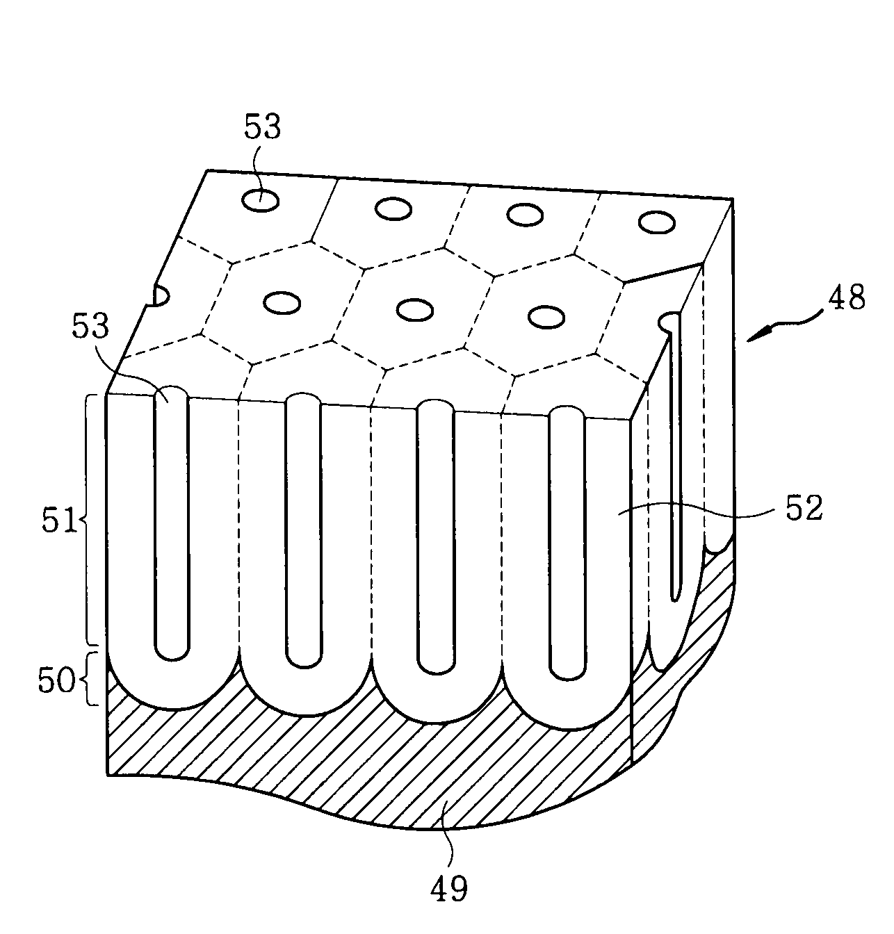
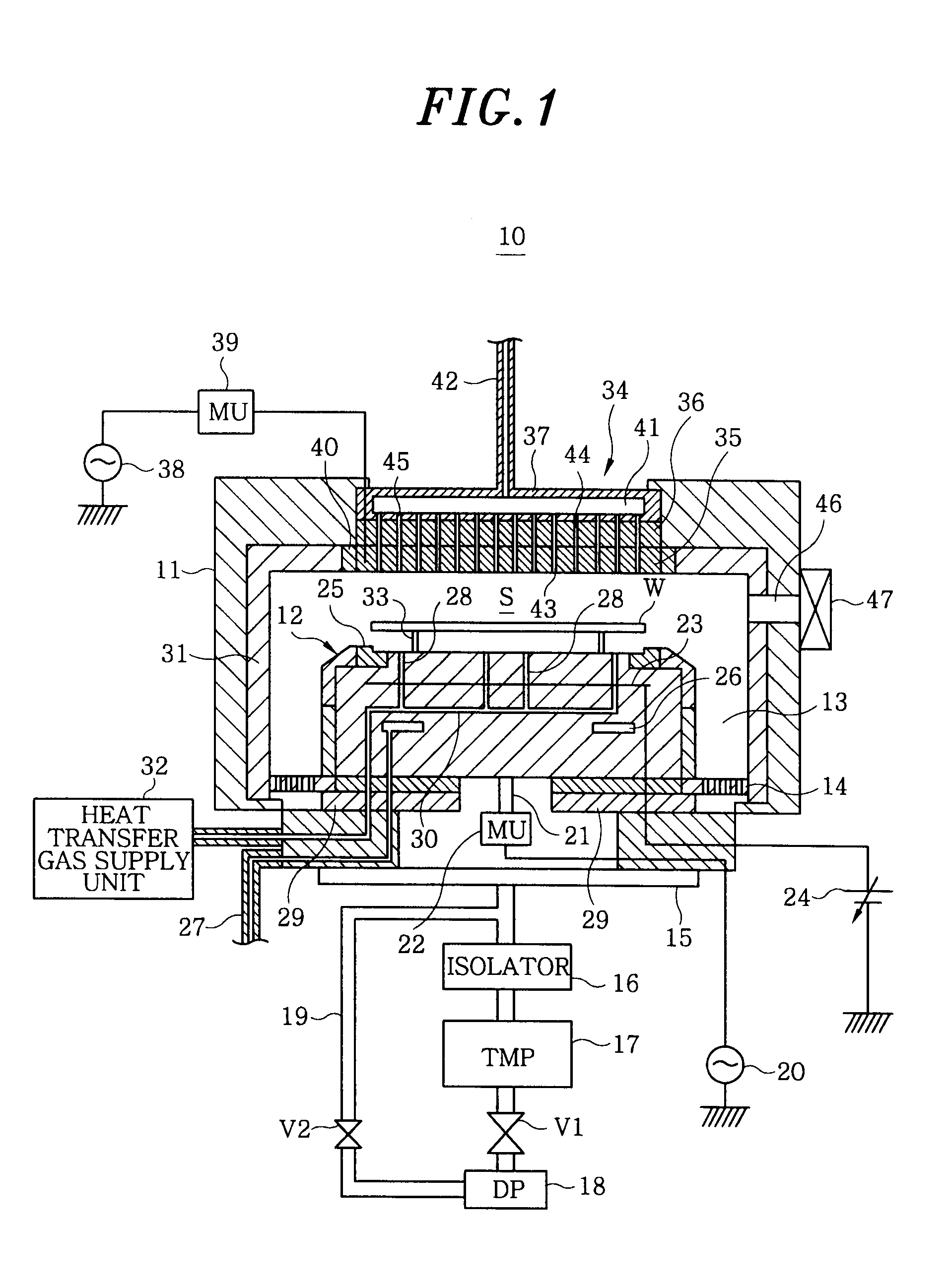
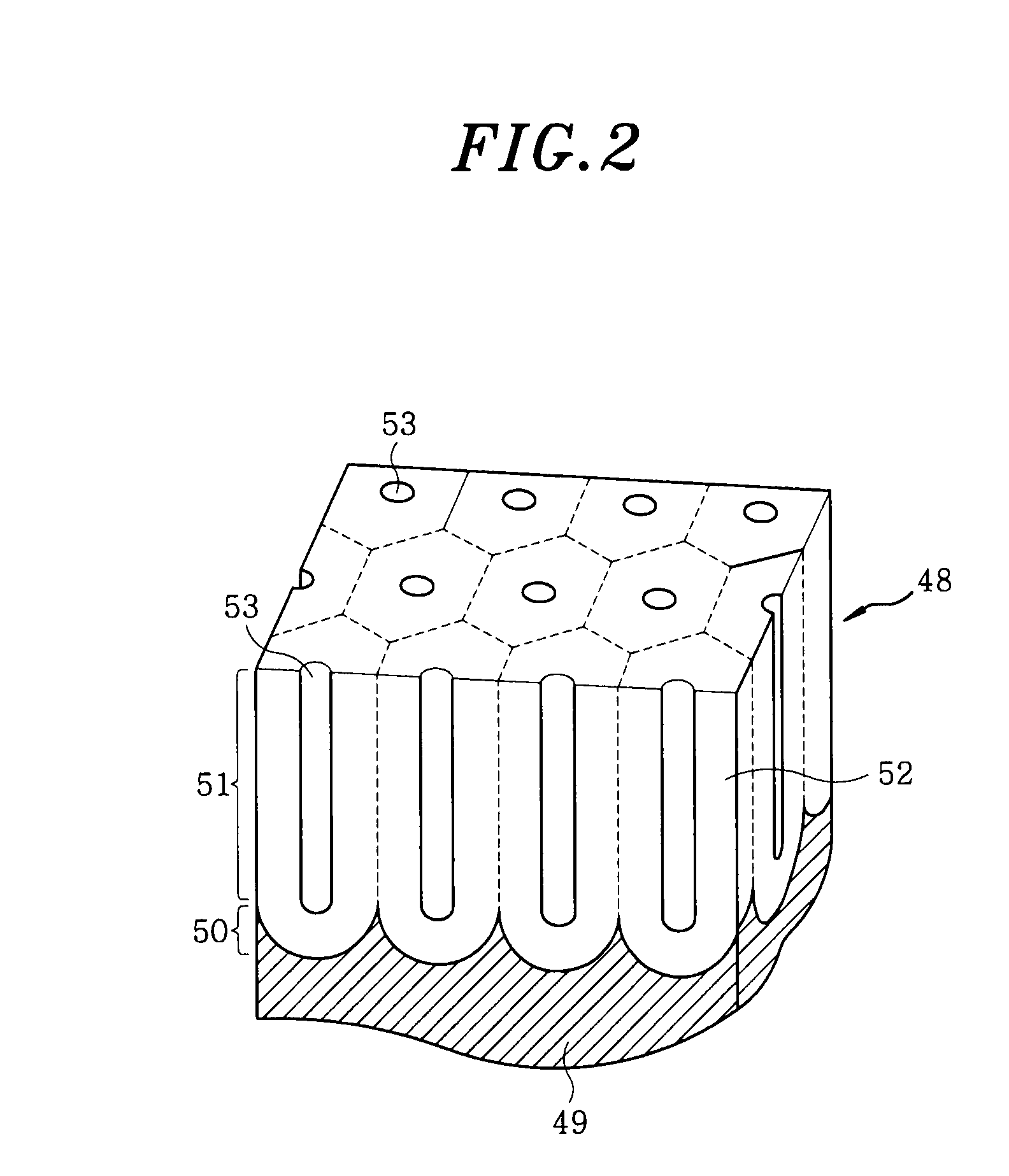
[0034]FIG. 1 is a cross-sectional view schematically showing a configuration of a substrate processing apparatus to which a component of a substrate processing apparatus in accordance with the embodiment of the present invention is applied. The substrate processing apparatus is configured to perform RIE (reactive ion etching) processing or ashing processing on a semiconductor wafer W as a substrate.

[0035]As shown in FIG. 1, a substrate processing apparatus 10 has a columnar chamber 11 which has a processing space S therein. In the chamber 11, a cylindrical susceptor 12 is disposed as a mounting table on which a semiconductor wafer (hereinaft...


PUM

PropertyMeasurementUnit
Percent by massaaaaaaaaaa
Massaaaaaaaaaa

Abstract

A component of a substrate processing apparatus that performs plasma processing on a substrate includes a base mainly formed of an aluminum alloy containing silicon. A film is formed on the surface of the base by an anodic oxidation process which includes connecting the component to an anode of a power supply and immersing the component in a solution mainly formed of an organic acid. The film is impregnated with ethyl silicate.

Description

FIELD OF THE INVENTION[0001]The present invention relates to a component of a substrate processing apparatus and a method for forming a film thereon, and more particularly to a component of a substrate processing apparatus that performs plasma processing on a substrate and a method for forming a film thereon.BACKGROUND OF THE INVENTION[0002]As substrate processing apparatuses for performing a predetermined processing on a wafer as a substrate, a film forming apparatus that performs film formation processing by CVD (chemical vapor deposition) or PVD (physical vapor deposition) and an etching apparatus that performs etching processing are known. In recent years, the substrate processing apparatus has increased in size with the increase in the diameter of wafer and, therefore, the increase in the weight of the substrate processing apparatus has become an issue to be concerned about. Thus, a lightweight aluminum member has been widely used as a material of components of the substrate pr...

Claims


Application Information

Patent Timeline
IPC IPC(8): B32B3/02B32B9/04C25D9/02
CPCC25D11/246Y10T428/218C25D11/005C25D21/02Y10T428/162C25D11/02H01L21/00C25D11/24
Inventor MITSUHASHI, KOJI
Owner TOKYO ELECTRON LTD
Why Eureka
Try Eureka