Reticle, and method of laying out wirings and vias

a technology of reticle and via, which is applied in the direction of photomechanical equipment, originals for photomechanical treatment, instruments, etc., can solve the problems of difficult to resolve the opening pattern of the via, the resist between the vias loses its shape, and the difficulty of forming the vias as designed in some cases, so as to improve the minimum distance, improve the reliability, and improve the product yield.

Active Publication Date: 2009-07-23
RENESAS ELECTRONICS CORP
View PDF7 Cites 4 Cited by
  • Summary
  • Abstract
  • Description
  • Claims
  • Application Information

AI Technical Summary

Benefits of technology

[0009]The present invention provides a reticle used for forming a plurality of vias for connecting a plurality of first wirings provided in a first wiring layer and a plurality of second wirings provided in a second wiring layer formed above the first wiring layer to each other, the plurality of first wirings and the plurality of second wirings being provided along one of a first direction and a second direction, the first direction and the second direction perpendicularly crossing each other, the reticle including a plurality of via opening patterns for forming the plurality of vias, in which: each of the plurality of via opening patterns has a rectangular shape; the plurality of via opening patterns are arranged to cause each side of each of the plurality of via opening patterns to be diagonal with respect to the first direction and the second direction; and a minimum distance between neighboring two of the plurality of via opening patterns, which are arranged diagonally with respect to the first direction and the second direction, is made to be larger, by rotating the plurality of via opening patterns with a center point of each of the plurality of via opening patterns being fixed, than a minimum distance between the plurality of via opening patterns when the plurality of via opening patterns are arranged to cause each side of each of the plurality of via opening patterns to be one of parallel to and perpendicular to the first direction and the second direction.
[0010]In the present invention, the wirings and the vias are arranged in a predetermined layout to obtain desired wiring density and degree of integration of vias. Further, the reticle according to the present invention has the via opening pattern in a predetermined shape. In this manner, the reticle can increase the minimum distance between the neighboring via opening patterns without lowering the degree of integration of the vias for connecting the wirings to each other. As a result, the reticle, which is capable of restraining the via shape from being deformed or the like and also restraining the occurrence of a short between the vias, is provided.
[0011]The present invention also provides a method of laying out wirings and vias, including: providing a plurality of first wirings in a first wiring layer; forming a plurality of the vias connected to the plurality of first wirings by light exposure using a reticle; and providing a plurality of second wirings to be connected to the plurality of vias in a second wiring layer different from the first wiring layer, in which: the plurality of first wirings and the plurality of second wirings are provided along one of a first direction and a second direction, the first direction and the second direction perpendicularly crossing each other; the reticle includes a plurality of via opening patterns for forming the plurality of vias; each of the plurality of via opening patterns has a rectangular shape; the plurality of via opening patterns are arranged to cause each side of each of the plurality of via opening patterns to be diagonal in plan view with respect to the first direction and the second direction; and a minimum distance between neighboring two of the plurality of via opening patterns, which are arranged diagonally with respect to the first direction and the second direction, is made to be larger, by rotating the plurality of via opening patterns with a center point of each of the plurality of via opening patterns being fixed, than a minimum distance between the plurality of via opening patterns when the plurality of via opening patterns are arranged to cause each side of each of the plurality of via opening patterns to be one of parallel to and perpendicular to the first direction and the second direction.
[0012]Further, the present invention provides a method of fabricating a semiconductor device using the reticle according to the present invention. The semiconductor device fabricated according to the present invention has improved product yield, reliability, and lifetime because the short between the vias is restrained and burying performance for the vias is improved.
[0013]By using the reticle and the method of laying out the wirings and the vias according to the present invention, a resolution of the via between the neighboring via opening patterns is improved even when the distance between the via opening patterns is smaller than a light wavelength used for light exposure at the time of light exposure. As a result, the deformation of the via shape can be restrained without lowering the degree of integration of the vias for connecting the wirings to each other. As a result, the short between the vias, which constitutes one of the reasons for failure during the operation of the semiconductor device, can be restrained. Moreover, the burying performance for the via is improved to improve the yield of products. Therefore, according to the present invention, the method of fabricating the semiconductor device with the improved yield, reliability, and lifetime is provided.

Problems solved by technology

On the other hand, if the degree of integration is increased by the miniaturization of an element, it becomes difficult to form the vias as designed in some cases.
If a large number of vias are provided to be close to each other in such a via arrangement, it becomes difficult to resolve a via opening pattern due to the increased degree of integration for the formation of the via opening pattern by light exposure using photolithography.
Moreover, even if the via opening pattern is resolved, a resist between the vias loses its shape to increase a frequency of occurrence of a short between the vias during an operation of the semiconductor device.
As a result, the short between the vias disadvantageously occurs in an area where the vias are formed at a high density, during the operation of the semiconductor device.
Further, the deformation of the via occurs to obstacle the burial of a wiring material.
If the distance between the via opening patterns is smaller than the light wavelength used for the light exposure, it becomes difficult to resolve the neighboring via opening patterns.
Therefore, as the via opening patterns become closer to each other, there is a point at which each of the via opening patterns is no longer satisfactorily resolved.
If the resolution is insufficient, there is a fear that even a part which is not desired to be dissolved is disadvantageously dissolved at the time of development of the via opening patterns on the resist after the light exposure.
As a result, the via shape is sometimes deformed to result in the occurrence of the short between the vias in the worst case.
Furthermore, when the via shape is deformed even if the via is successfully resolved, there is a fear that an initial breakdown voltage during the operation of the semiconductor device may be lowered.
Therefore, even when the vias are arranged as illustrated in FIG. 5, there still exist the problems such as the via deformation and the occurrence of the short between the vias which constitutes one of the reasons for failure occurring during the operation of the semiconductor device.
Therefore, there is a fear that incomplete burial of the via or a reduction in yield of products may be brought about.
On the other hand, when the distance between the vias is increased, there arises another problem of a lowered degree of integration of the vias.

Method used


Image

  • Reticle, and method of laying out wirings and vias
  • Reticle, and method of laying out wirings and vias
  • Reticle, and method of laying out wirings and vias

Examples


example 1

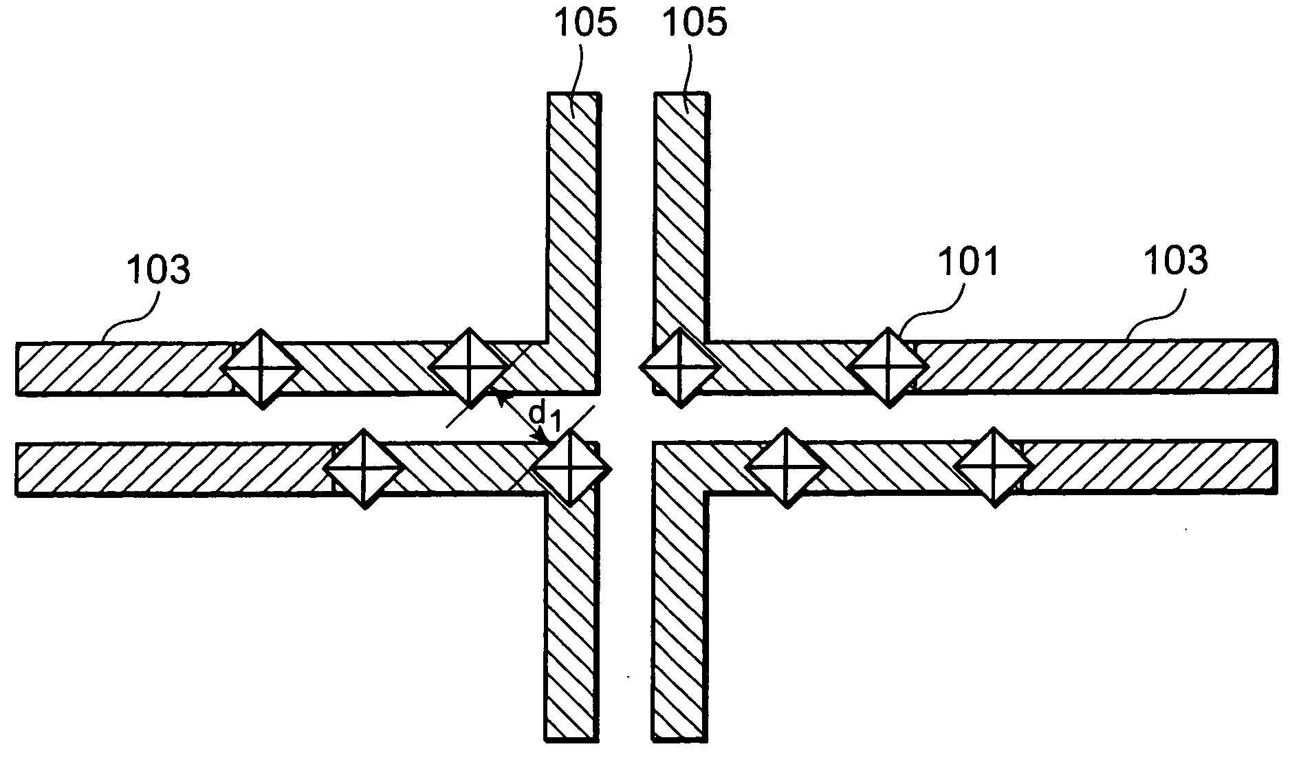
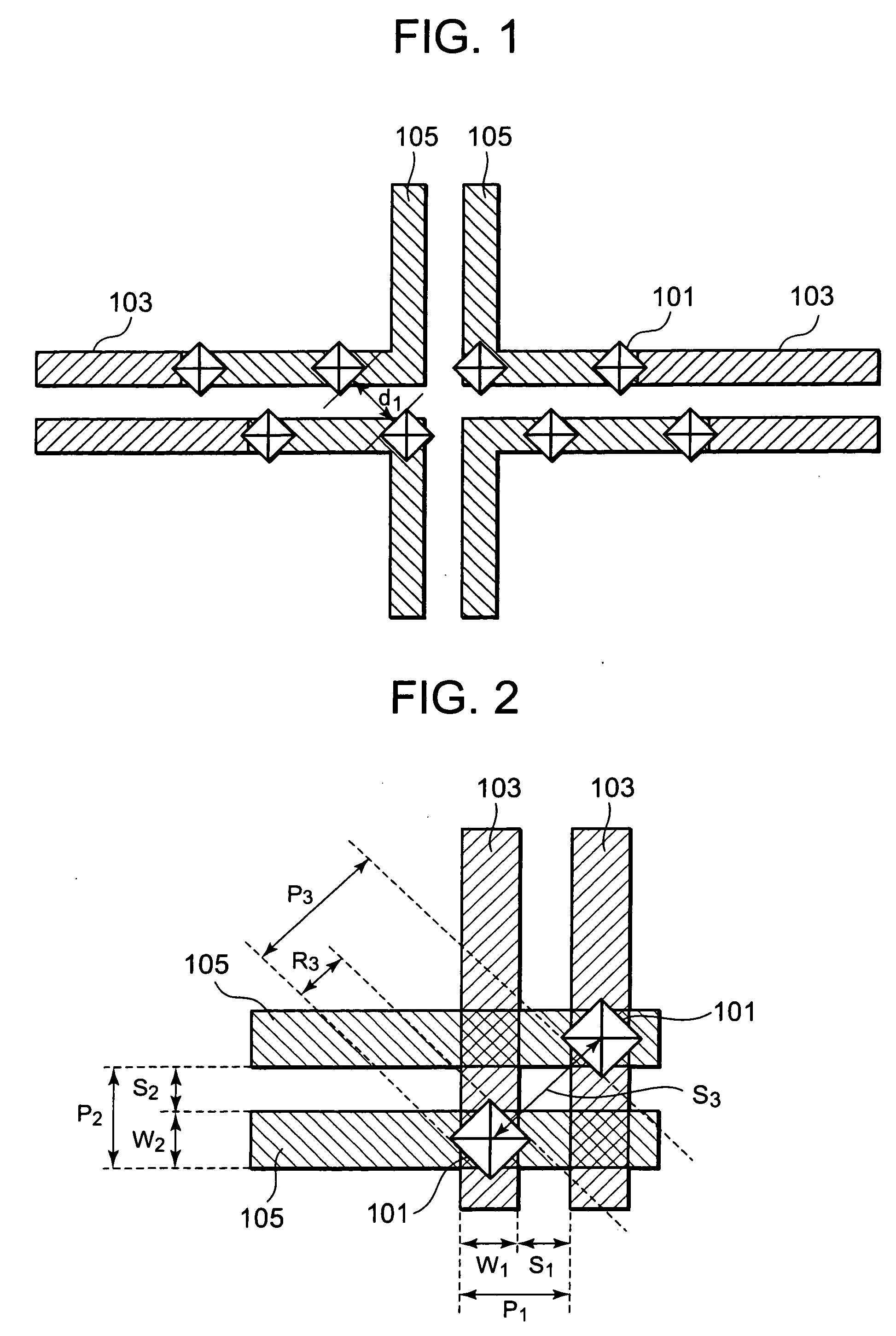
[0053]The via holes were formed by the photolithography using the layout of the wirings and the vias, which is illustrated in FIG. 1. The conditions used in this Example 1 were as follows. The shape of the via opening pattern was square. The minimum distance d1 between the neighboring via opening patterns was expressed by: (2×21 / 2−1)×S, where S is the distance between the wirings.

[0054]As specific conditions, the distance S between the wirings was 70 nm, the wiring width W was 70 nm, the wiring pitch P was 140 nm, the length R of each of the sides of the via opening pattern was 70 nm, and the angle of each of the sides of the via opening pattern with respect to the wiring was 45 degrees or 135 degrees. In this arrangement, the minimum distance d1 between the neighboring via opening patterns was: (2×21 / 2−1)×S=128 nm. The light wavelength (λ) for the light exposure was 193 nm.

[0055]The shape of the via hole formed after the photolithography was circular. The occurrence of the linkage ...

example 2

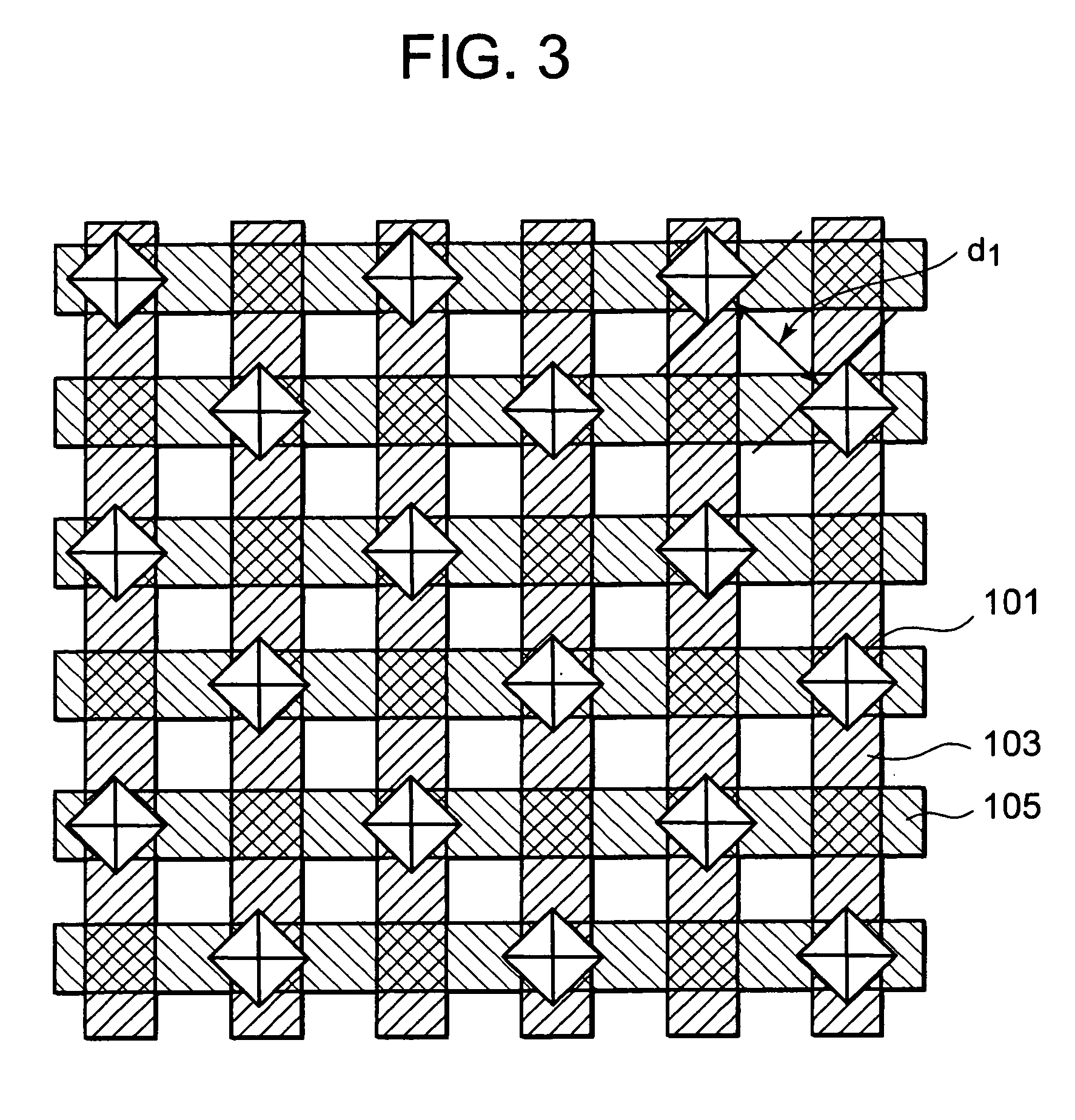
[0056]The via holes were formed by the photolithography using the layout of the wirings and the vias, which is illustrated in FIG. 3. This Example 2 is the same as Example 1 except that the first wirings 103 and the second wirings 105 were arranged to perpendicularly cross each other. The conditions used in this Example 2 were the same as those used in Example 1. Therefore, the minimum distance d1 between the neighboring via opening patterns was: (2×21 / 2−1)×S, where S is the distance between the wirings, and was obtained as 128 nm.

[0057]The shape of the via hole formed after the photolithography was circular. The occurrence of the linkage between the vias was not observed. Therefore, good via holes were formed.


PUM

PropertyMeasurementUnit
angleaaaaaaaaaa
angleaaaaaaaaaa
lengthaaaaaaaaaa

Abstract

Provided is a reticle used for forming a plurality of vias for connecting first wirings provided in a first wiring layer and second wirings provided in a second wiring layer formed above the first wiring layer. The first wirings and the second wirings are provided along one of a first direction and a second direction, and the first direction and the second direction perpendicularly cross each other. The reticle includes a plurality of via opening patterns for forming the plurality of vias. Each of the plurality of via opening patterns has a rectangular shape, and is arranged to cause each side of each of the via opening patterns to be diagonal with respect to the first direction and the second direction.

Description

BACKGROUND OF THE INVENTION[0001]1. Field of the Invention[0002]The present invention relates to a reticle, and a method of laying out wirings and vias.[0003]2. Description of the Related Art[0004]Recently, with the miniaturization of semiconductor devices, there is a demand for reduction in a distance between wirings to increase a wiring density (see Japanese Patent Application Laid-open No. 2005-19604; hereinafter, referred to as Patent Document 1). In response to such a demand, it is necessary to increase a degree of integration even for vias which are formed for the connection between the wirings in upper and lower wiring layers. On the other hand, if the degree of integration is increased by the miniaturization of an element, it becomes difficult to form the vias as designed in some cases.[0005]FIG. 4 illustrates an example of a conventional method of laying out the wirings and the vias. In FIG. 4, a first wiring layer including first wirings 103 and a second wiring layer inclu...

Claims


Application Information

Patent Timeline
Patent Type & Authority Applications(United States)
IPC IPC(8): G03F1/00G03F7/20G03F1/70H01L21/027H01L21/3205H01L21/768H01L21/82H01L23/522
CPCG03F1/14G03F1/144G03F1/36H01L21/31144H01L21/76816H01L2924/0002H01L23/5226H01L23/528H01L2924/00G03F1/00
Inventor KUNISHIMA, HIROYUKI
Owner RENESAS ELECTRONICS CORP
Why Eureka
Try Eureka