Anneal sequence integration for CMOS devices

a technology of cmos and anneal sequence, which is applied in the direction of semiconductor/solid-state device manufacturing, basic electric elements, electric apparatus, etc., can solve the problems of low dopant diffusion, difficult balance maintenance, and high dopant activation with little dopant diffusion

Inactive Publication Date: 2009-07-23
IBM CORP
View PDF6 Cites 8 Cited by
  • Summary
  • Abstract
  • Description
  • Claims
  • Application Information

AI Technical Summary

Benefits of technology

[0001]The present invention relates to semiconductor devices, and more particularly to a method for forming a complementary metal-oxide semiconductor (CMOS) device, the method comprising a firs

Problems solved by technology

Ultra shallow source/drain (S/D) junctions are becoming more challenging to produce as junction depth is required to be less than 30 nm for sub-100 nm CMOS devices.
Activating the polysilicon gate electrode without causing dopant diffusion is a major challenge for front end of line (FEOL)

Method used


Image

  • Anneal sequence integration for CMOS devices
  • Anneal sequence integration for CMOS devices
  • Anneal sequence integration for CMOS devices

Examples


Embodiment Construction

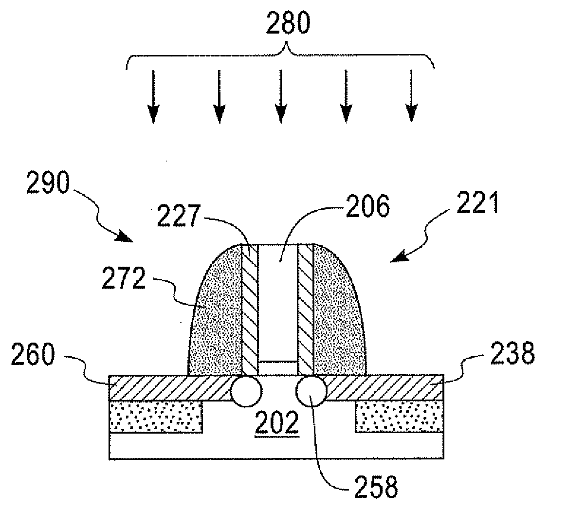
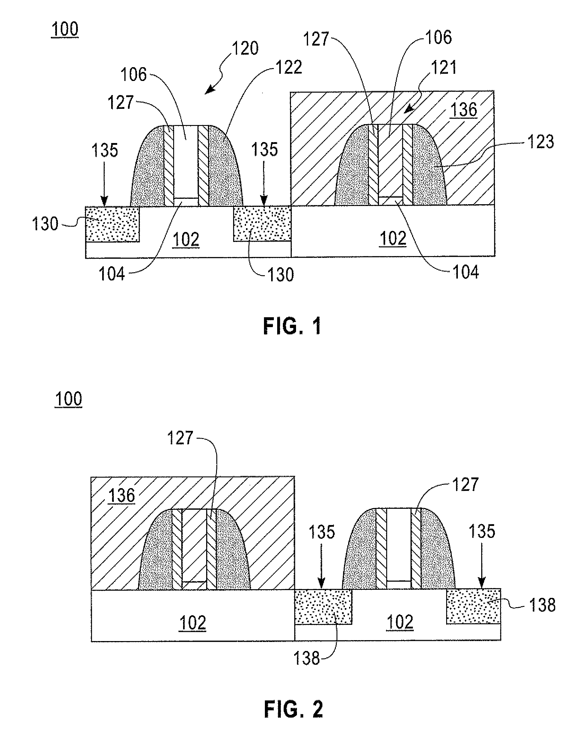
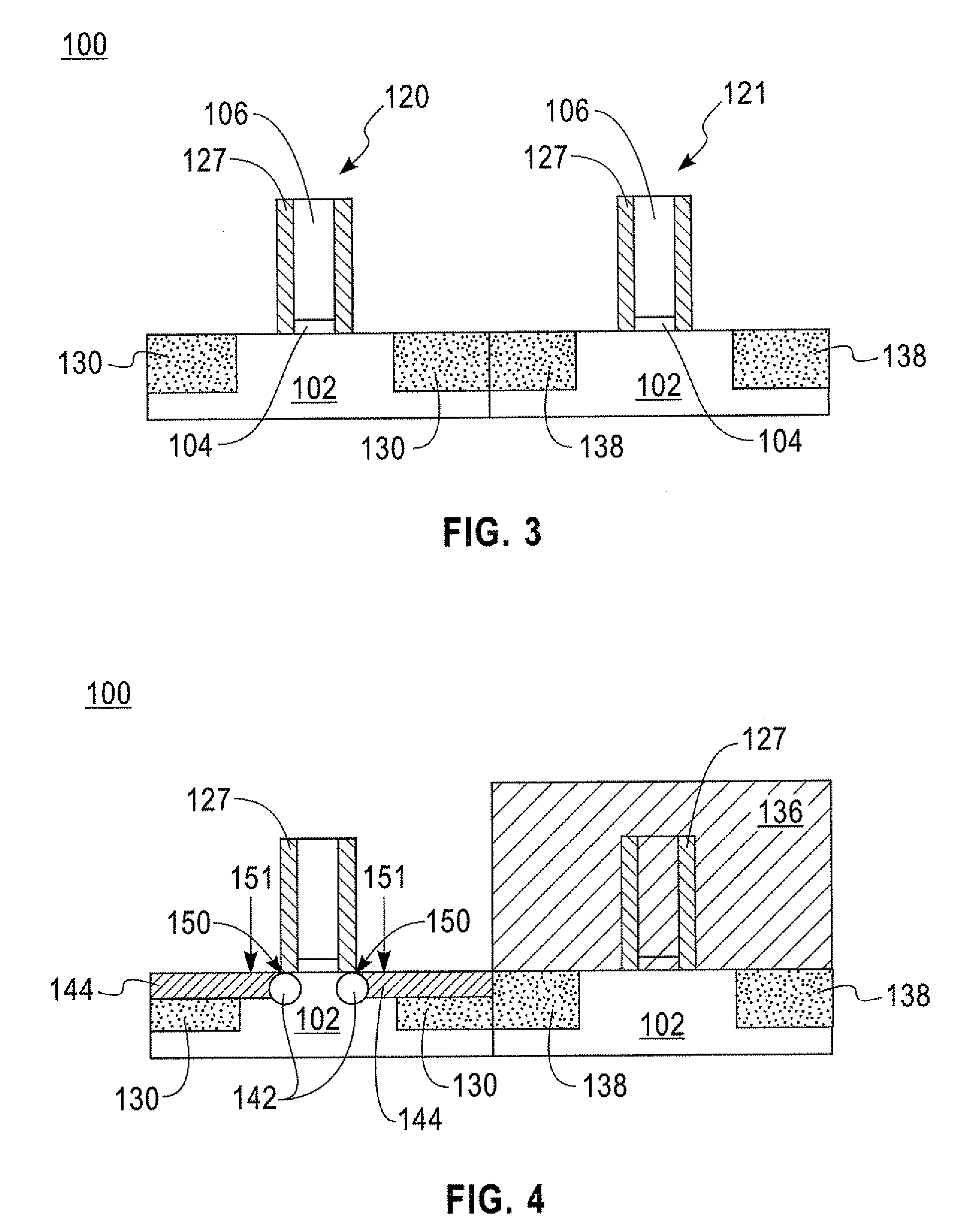
[0056]The present invention, which provides a method for forming a CMOS device, will now be described in greater detail by referring to the drawings that accompany the present application. It is noted that the drawings of the present application are provided for illustrative purposes and are thus not drawn to scale. Moreover, like and corresponding elements shown in the drawings are referred to by like reference numerals.

[0057]Reference is first made generally to FIGS. 1-8, which are cross sectional views of a structure 100 during various stages of an embodiment of the present invention. Although the drawings show the presence of a pair of gates (i.e., a CMOS transistor structure with PFET and NFET transistors), the present invention is not limited to that number of gates. Instead, the present integration process works for any number of gates. Hence, a plurality of gates may be present across a single semiconductor structure. Furthermore, it is noted that the semiconductor structure...


PUM


Abstract

The present invention relates to semiconductor devices, and more particularly to a method for forming a CMOS semiconductor device, the method including a first integration anneal sequence for each NFET and a second integration anneal sequence for each PFET of the semiconductor device. The method includes providing a structure having an nFET gate stack and a pFET gate stack patterned on a substrate. A first disposable spacer is formed adjacent the nFET gate stack and a second disposable spacer is formed adjacent the pFET gate stack. A first doped S/D region and a second doped S/D region are then formed in the substrate. The first and second disposable spacers are removed after the first and second doped S/D regions are formed. A first halo implant and a first S/D extension region are formed adjacent the nFET gate stack after the first and second disposable spacers are removed. The structure is annealed using a RTA process. A first final spacer adjacent the nFET gate stack and the second final spacer adjacent the pFET gate stack are then formed after a second halo implant and a second S/D extension region are formed adjacent the pFET. The structure is annealed using a laser anneal process to form an NFET and a PFET on the substrate.

Description

FIELD OF THE INVENTION[0001]The present invention relates to semiconductor devices, and more particularly to a method for forming a complementary metal-oxide semiconductor (CMOS) device, the method comprising a first integration anneal sequence for each n-type field effect transistor (NFET) and a second integration anneal sequence for each p-type field effect transistor (PFET) of the semiconductor device.BACKGROUND OF THE INVENTION[0002]As smaller transistors are manufactured, thinner gate dielectric materials are needed to enhance device performance. Ultra shallow source / drain (S / D) junctions are becoming more challenging to produce as junction depth is required to be less than 30 nm for sub-100 nm CMOS devices. Activating the polysilicon gate electrode without causing dopant diffusion is a major challenge for front end of line (FEOL) processing. Conventional processes for activating the polysilicon gate electrode include a rapid thermal annealing (RTA) process. A tight balance exi...

Claims


Application Information

Patent Timeline
IPC IPC(8): H01L21/8238
CPCH01L21/823807H01L21/823864H01L21/823814
Inventor LEE, KAM-LEUNGKOZLOWSKI, PAUL M.
Owner IBM CORP
Why Eureka
Try Eureka