Nanotube array electronic and opto-electronic devices

a technology of carbon nanotubes and arrays, applied in the field of carbon nanotube arrays of pand nchannel transistors and pn diodes, can solve the problems of preventing any possibility of ic mass manufacturing, impracticality for any scale of circuit integration, etc., and achieves unique speed of operation, minimize contact resistance, and low contact resistance

Inactive Publication Date: 2009-07-30
NANO ELECTRONICS & PHOTONIC DEVICES & CIRCUITS
View PDF31 Cites 21 Cited by
  • Summary
  • Abstract
  • Description
  • Claims
  • Application Information

AI Technical Summary

Benefits of technology

[0018]Similar planar multilayer deposition technique is applied for fabrication of a new nanotube array bipolar transistor (NABT) of p-n-p and n-p-n device configurations, the change in the type of conductivity in the middle of the nanotube (transistor base) being produced using the described above methods of annealing in vacuum or in appropriate gas atmosphere. The contact to the base will be made using the same method of deposition of the metal layer sandwiched between two dielectrics, similar to the gate in the CMIN. Unlike the insulated gate of the CMIN, however, the metal in the NABT is directly attached to the nanotube sidewall to provide the base contact with a low contact resistance. To minimize the contact resistance, Pd as a contact metal is preferable, see A. Javey et a

Problems solved by technology

The drawback of this method is its impracticality for any scale of circuit integration: placement of multiple identical nanotubes to enhance the

Method used


Image

  • Nanotube array electronic and opto-electronic devices
  • Nanotube array electronic and opto-electronic devices
  • Nanotube array electronic and opto-electronic devices

Examples


Embodiment Construction

[0026]1. Design and Fabrication of CMIN

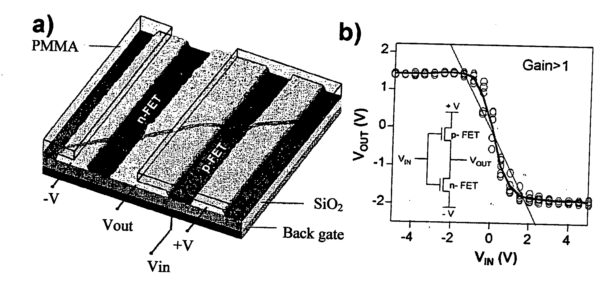
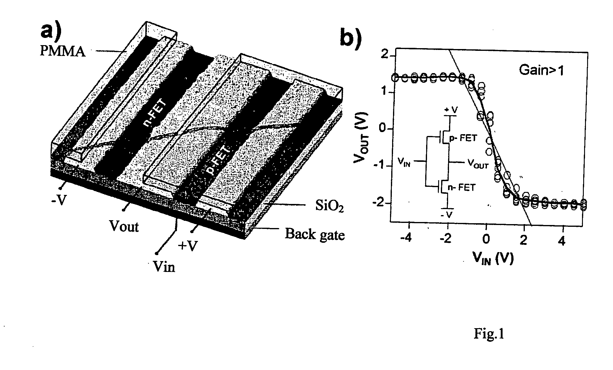
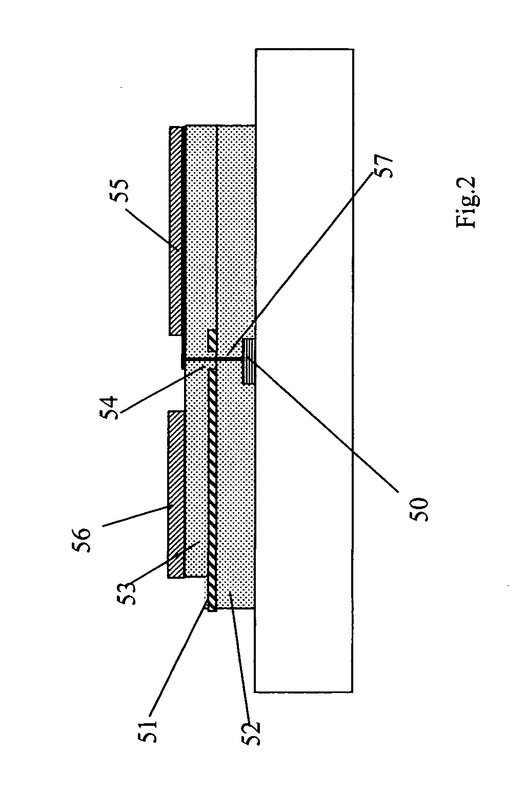
[0027]In the CMIN design, shown in FIG. 3a, two arrays of the nanotubes 31 and 32 are grown on two separate metal electrodes 33 and 34 normally to the substrate 30, which can be glass plate or Si wafer or any other dielectric substrate capable of sustaining nanotube growth temperatures (˜600° C.). The nanotube arrays have different types of conductivity, which are produced using above discussed methods of the type conversion. Let as assume that nanotubes 31 are p-type and nanotubes 32 are n-type, although reverse type assignment is equally applicable, since the CMIN structure is symmetrical. The metal layer 35 sandwiched between two dielectric layers 36 and 37 represents a common gate for two transistors, wherein the first transistors comprises the substrate metal 33 as a source, the nanotube array 31 as a conducting p-channel and the top metal layer 38 as a drain, while the same top metal layer 38 is a source of the second transistor, the nano...


PUM


Abstract

Carbon nanotube (CNT)-based devices and technology for their fabrication are disclosed. The discussed electronic and photonic devices and circuits rely on the nanotube arrays grown on a variety of substrates, such as glass or Si wafer. The planar, multiple layer deposition technique and simple methods of change of the nanotube conductivity type during the device processing are utilized to provide a simple and cost effective technology for a large scale circuit integration. Such devices as p-n diode, CMOS-like circuit, bipolar transistor, light emitting diode and laser are disclosed, all of them are expected to have superior performance then their semiconductor-based counterparts due to excellent CNT electrical and optical properties. When fabricated on Si-wafers, the CNT-based devices can be combined with the Si circuit elements, thus producing hybrid Si-CNT devices and circuits.

Description

FIELD OF THE INVENTION[0001]The invention relates to carbon nanotube array of p- and n-channel transistors and p-n diodes and specifically, to complementary circuits of nanorube array field-effect transistors as well as bipolar transistors and optoelectronic devices.BACKGROUND OF THE INVENTION[0002]The Carbon Nanotubes (CNT) are viewed to be a new key element for future electronics. In the CNT, such unique properties as quantization of the electron spectrum, ballistic electron propagation along the tube, current densities as high as 109 A / cm2, existence of the semiconductor phase, possibilities for n- and p-doping with a high carrier mobilities, as well as excellent thermal conductance, make the nanotubes a great candidate for future novel high-speed, high efficiency electronic and photonic devices.[0003]The key element widely used in the electronic logic circuits is CMOS, wherein both switching states consume minimum energy, see. e.g. J. R. Brews in High-speed Semiconductor Devices...

Claims


Application Information

Patent Timeline
IPC IPC(8): H01L29/06
CPCB82Y10/00H01L27/283H01L51/057H01L51/0558H01L51/0048H10K19/10H10K85/221H10K10/491H10K10/484
Inventor KASTALSKY, ALEXANDER
Owner NANO ELECTRONICS & PHOTONIC DEVICES & CIRCUITS
Why Eureka
Try Eureka