Capacitor and method of manufacturing the same

a technology of capacitors and dielectric components, applied in the manufacture of electrolytic capacitors, capacitor dielectric layers, fixed capacitor details, etc., can solve the problems of increasing capacitance, reducing the degree of freedom causing liquid leakage, etc., so as to improve the facultativity of electrode metal materials, the manufacturing process can be simplified, and the effect of increasing the capacitance density

Active Publication Date: 2009-08-06
TAIYO YUDEN KK
View PDF2 Cites 22 Cited by
  • Summary
  • Abstract
  • Description
  • Claims
  • Application Information

AI Technical Summary

Benefits of technology

[0008]At least one of the disclosed embodiments of the present invention has been implemented in view of the foregoing attention, and has an object to provide a capacitor whose capacitance density can be enhanced, and a method of manufacturing the capacitor. Furthermore, at le

Problems solved by technology

The Al electrolytic capacitors have a problem that liquid leak, etc. occurs due to use of electrolytic liquid, etc.
Furthermore, the laminated ceramic capacitors require a burning step, and thus it induces thermal shrinkage between an electrode and a dielectric member, etc.
First, in the technique of the JP-B-Sho-61-29133, the semiconductor grain boundary insulation type dielectric ceramic having plural through holes is used as the dielectric layer, and it has a structure that the capacitance electrode members are selectively inserted in the respective through holes. However, the microfabrication is difficult, and it is difficult to increase the capacitance by increasing

Method used


Image

  • Capacitor and method of manufacturing the same
  • Capacitor and method of manufacturing the same
  • Capacitor and method of manufacturing the same

Examples


first embodiment

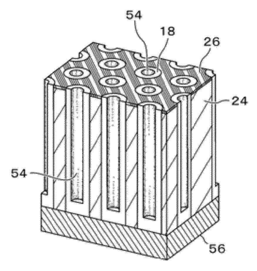
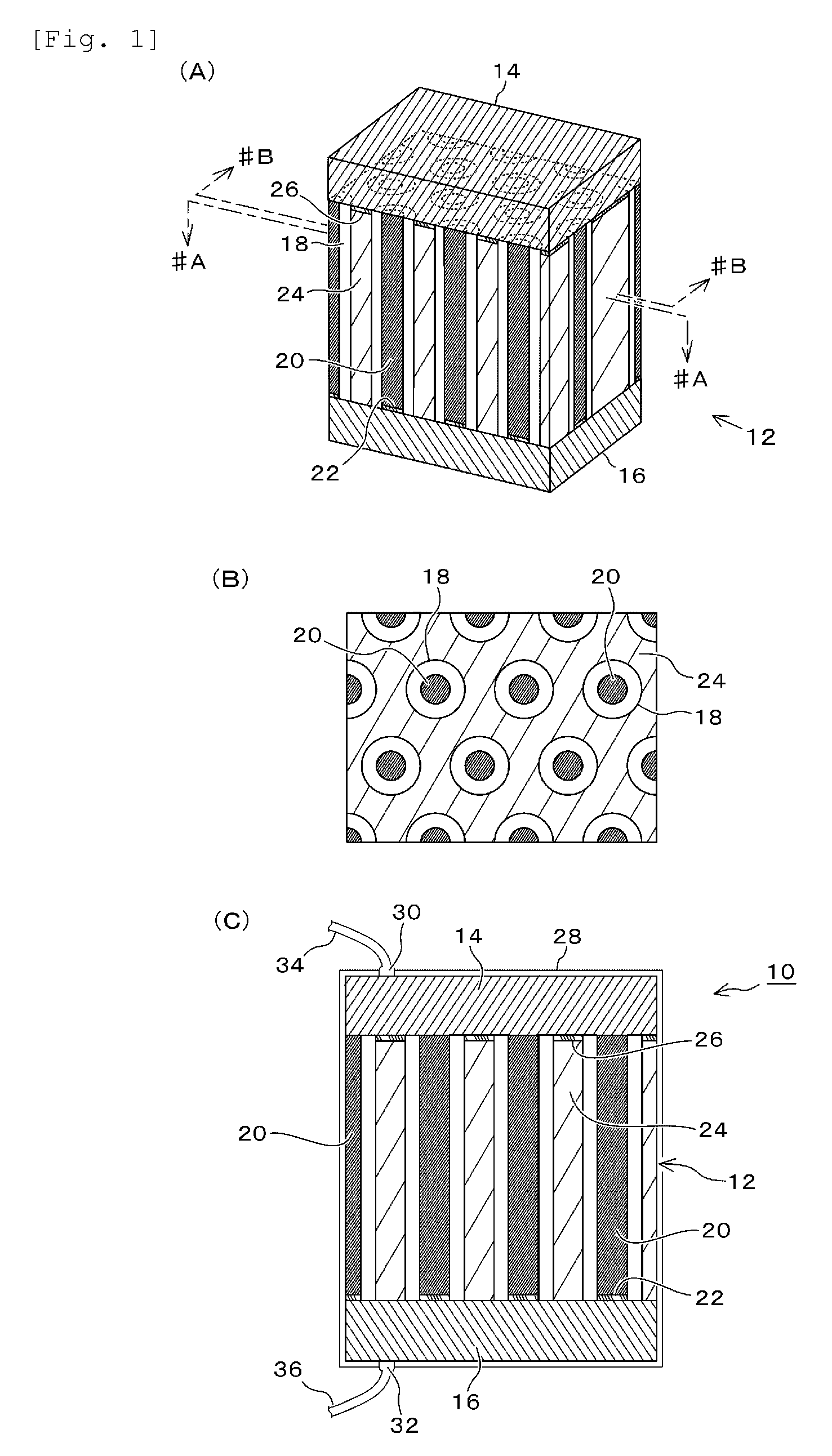
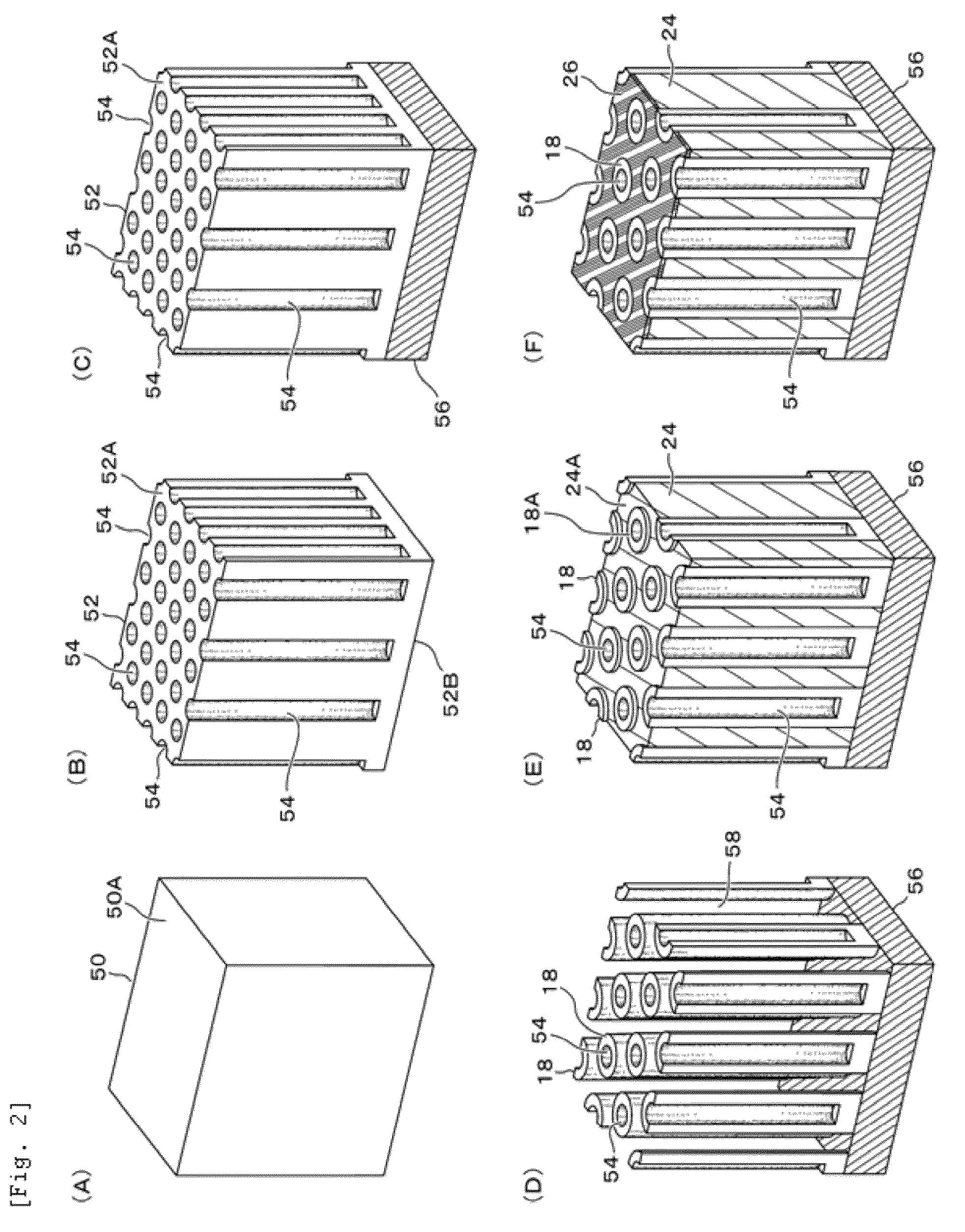
[0027]First, a first embodiment according to the present invention will be described with reference to FIGS. 1A to 4F. FIG. 1A is a perspective view showing the outlook of a capacitor element according to the first embodiment of the present invention, FIG. 1B is a cross-sectional view of the capacitor element which is taken along a #A-#A line of FIG. 1A and viewed in a direction of an arrow, and FIG. 1C is a cross-sectional view of a capacitor of this embodiment and also is a cross-sectional view which is taken along #B-#B line of FIG. 1A and viewed in a direction of an arrow, FIGS. 2A to 3F are diagrams showing examples of a manufacturing process according to the first embodiment, and FIGS. 4A and 4B are schematic diagrams showing cross-sectional shapes of electrode structures of the first embodiment and a comparative example.

[0028]The capacitor 10 according to this embodiment is mainly constructed by a capacitor element 12 as shown in FIGS. 1A to 1C. The capacitor element 12 compr...

second embodiment

[0042]Next, a second embodiment according to the present invention will be described with reference to FIGS. 5 to 7. The same / corresponding constituent elements as / to the above-described embodiment are represented by the same reference numerals. FIG. 5 is a cross-sectional view showing the main part of a capacitor element according to this embodiment, and FIGS. 6A to 7D are diagrams showing an example of the manufacturing process of this embodiment. In this embodiment, as shown in the cross-sectional view of FIG. 5, an air gap 102 is formed between the tip of the first electrode 20 and the electrically conductive layer 16, and also an air gap 104 is formed between the tip of the second electrode 24 and the electrically conductive layer 14. The insulation is established by the air gaps 102 and 104, thereby allocating the electrodes. This basic structure is the same as the first embodiment.

[0043]Next, a manufacturing method according to this embodiment will be described with reference...


PUM

PropertyMeasurementUnit
Electrical conductivityaaaaaaaaaa
Aspect ratioaaaaaaaaaa
aaaaaaaaaa

Abstract

A capacitor includes a pair of electrically conductive layers; a plurality of substantially or nearly tubular dielectric materials disposed between the pair of electrically conductive layers formed of anodic oxide of metal; first electrodes which are filled in hollow portions of the dielectric materials and connected to one of the electrically conductive layers; and a second electrode that is filled in voids between the respective dielectric materials and connected to the other electrically conductive layer.

Description

BACKGROUND OF THE INVENTION[0001]1. Field of the Invention[0002]The present invention relates to a capacitor and a method of manufacturing the same, and particularly to enhancement of capacitance density, enhancement of facultativity of electrode metal and simplification of a manufacturing process.[0003]2. Description of the Related Art[0004]Al electrolytic capacitors and laminated ceramic capacitors are known as capacitors which are broadly used at present. The Al electrolytic capacitors have a problem that liquid leak, etc. occurs due to use of electrolytic liquid, etc. Furthermore, the laminated ceramic capacitors require a burning step, and thus it induces thermal shrinkage between an electrode and a dielectric member, etc. For example, as a technique of implementing a compact and large-capacitance capacitor is known a grain boundary insulating type semiconductor magnetic capacitor disclosed in JP-B-Sho-61-29133, and a capacitor structure and a manufacturing method thereof discl...

Claims


Application Information

Patent Timeline
IPC IPC(8): H01G4/20H01G7/00
CPCH01G9/0032H01G9/048Y10T29/435H01G9/14H01G9/07
Inventor MASUDA, HIDETOSHIKUROSAWA, MASARUMIZUNO, KOTARO
Owner TAIYO YUDEN KK
Why Eureka
Try Eureka