

Vertical cavity surface emitting laser
a laser and vertical cavity technology, applied in semiconductor lasers, laser details, optical resonator shape and construction, etc., can solve the problem of difficult high laser output, and achieve the effect of simple construction
- Summary
- Abstract
- Description
- Claims
- Application Information
AI Technical Summary
Benefits of technology
Problems solved by technology
Method used
Image

Examples
example 1
[0182]Example 1 describes a constitution of a vertical cavity surface emitting laser of the present invention.
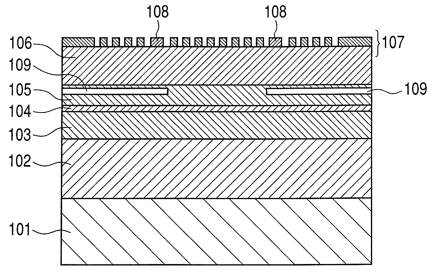
[0183]FIG. 7 illustrates schematically a cross-section of the vertical cavity surface emitting laser of this Example. In FIG. 7, the reference numerals denote the followings: 701, a substrate; 702, a DBR mirror; 703, a lower cladding layer; 704, an active layer; 705, an upper cladding layer; 706, an upper spacer layer; 707, a photonic crystal mirror; 708, a phase-shift part; 709, an oxidation-formed confining layer; 710, an air-bridge structure; 711, an n-electrode; and 712, a p-electrode.
[0184]In this Example, DBR mirror 702 is formed on substrate 701.
[0185]DBR mirror 702 is formed by alternate lamination of lower refractive-index layers and higher refractive-index layers of an optical thickness of λ / 4.
[0186]The lower refractive-index layer is formed from n-Al0.12Ga0.88As, and the higher refractive-index layer is formed from n-Al0.9Ga0.1As. The number of the pairs of the lo...
example 2
[0221]This Example 2 describes a constitution of another vertical cavity surface emitting laser different from that of Example 1.
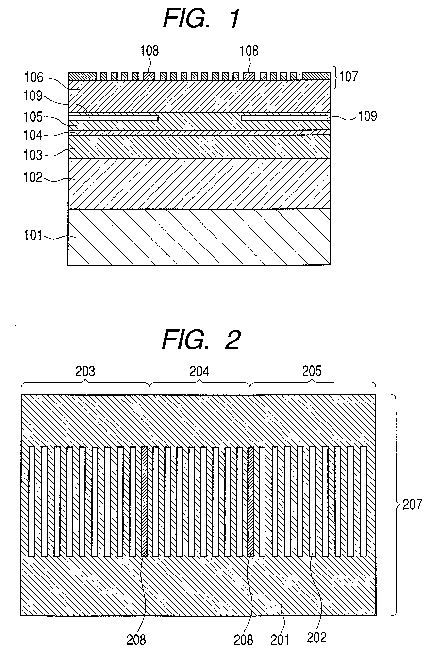
[0222]FIG. 11 illustrates a schematic sectional view of the vertical cavity surface emitting laser of this Example. In FIG. 11, the reference numerals denote the followings: 1101, a substrate; 1102, a DBS mirror; 1103, a lower cladding layer; 1104, an active layer; 1105, an upper cladding layer; 1106, an upper spacer layer; 1107, a photonic crystal mirror; 1108, a phase-shift part; 1109, an oxidation-formed confining layer; 1110, an air-bridge structure; 1111, an n-electrode; and 1112, a p-electrode.
[0223]In this Example 2, being different from Example 1, phase-shift parts 1108 are placed at the positions different from the positions in Example 1 in the photonic crystal mirror plane direction, and are formed in the adjacent layer, not within the inside of the photonic crystal layer 1107.
[0224]Specifically, phase-shift parts 1108 are placed on the positions...
example 3
[0243]This Example 3 describes a constitution of a vertical cavity surface emitting laser which employs a two-dimensional photonic crystal as the photonic crystal mirror.
[0244]FIG. 14 is a schematic plan view of the photonic crystal mirror of the vertical cavity surface emitting laser in Example 3 of the present invention.
[0245]In FIG. 14, the reference numerals denote the followings: 1401, a photonic crystal layer, 1402, a hole; 1403, a phase-shift part; and 1404, a p-electrode.
[0246]In Example 3, the constitution and materials of the laser device are basically the same as those in Example 1 except that the pattern of the employed photonic crystal mirror is two-dimensional.
[0247]In this Example, as illustrated in FIG. 14, circular holes 1402 are provided periodically in photonic crystal layer 1401 to form a two-dimensional crystal of a tetragonal lattice.
[0248]The phase-shift portion is placed inside by three periods from the end of the photonic crystal region.
[0249]The photonic cr...
PUM
 Abstract
Description
Claims
Application Information