Optical Integrated Circuit, Opto-Electronic Integrated Circuit and Manufacturing Method Thereof

Inactive Publication Date: 2009-08-06
NEOPHOTONICS SEMICON GK
View PDF10 Cites 2 Cited by
  • Summary
  • Abstract
  • Description
  • Claims
  • Application Information

AI Technical Summary

Benefits of technology

[0021]According to the first and second inventions, since the sapphire substrate is used as the lower clad of the optical waveguide and silicon is used as the core of the optical waveguide, a sufficient difference in refractive index can be obtained. Therefore, the size of the core can be reduced. Thus, since the number of processes for fabricating the core and the time required to fabricate the core can be cut down, and yields can be improved, an optical integrated circuit can be provided at low cost. According to the third and fourth inventions,

Problems solved by technology

When, however, the opto-electronic integrated circuit is fabricated using the conventional planar lightwave circuit, the following drawbacks occur.
When the planar lightwave circuit and the semiconductor integrated circuit are formed on the silicon substrate on a hybrid or monolithic basis, such a conventional planar lightwave circuit as mentioned above has the drawback that parasitic capacitance produced in the semiconductor integrated circuit increases.
Therefore, the opto-electronic integrated circuit using the silicon substrate is not capable of obtaining sufficient characteristics upon a high-speed operation of 1 Gbyte/second or more.
It was therefore difficult to use it in applications such as high-speed optical communications.
While the optical waveguide can be formed even on the glass substrate as described above, the fabrication of the semiconductor integrated circuit for the high-speed optical communications on the glass substrate is difficult for techniques under the present situation due to crystallizability, temperatures and

Method used


Image

  • Optical Integrated Circuit, Opto-Electronic Integrated Circuit and Manufacturing Method Thereof
  • Optical Integrated Circuit, Opto-Electronic Integrated Circuit and Manufacturing Method Thereof
  • Optical Integrated Circuit, Opto-Electronic Integrated Circuit and Manufacturing Method Thereof

Examples


first preferred embodiment

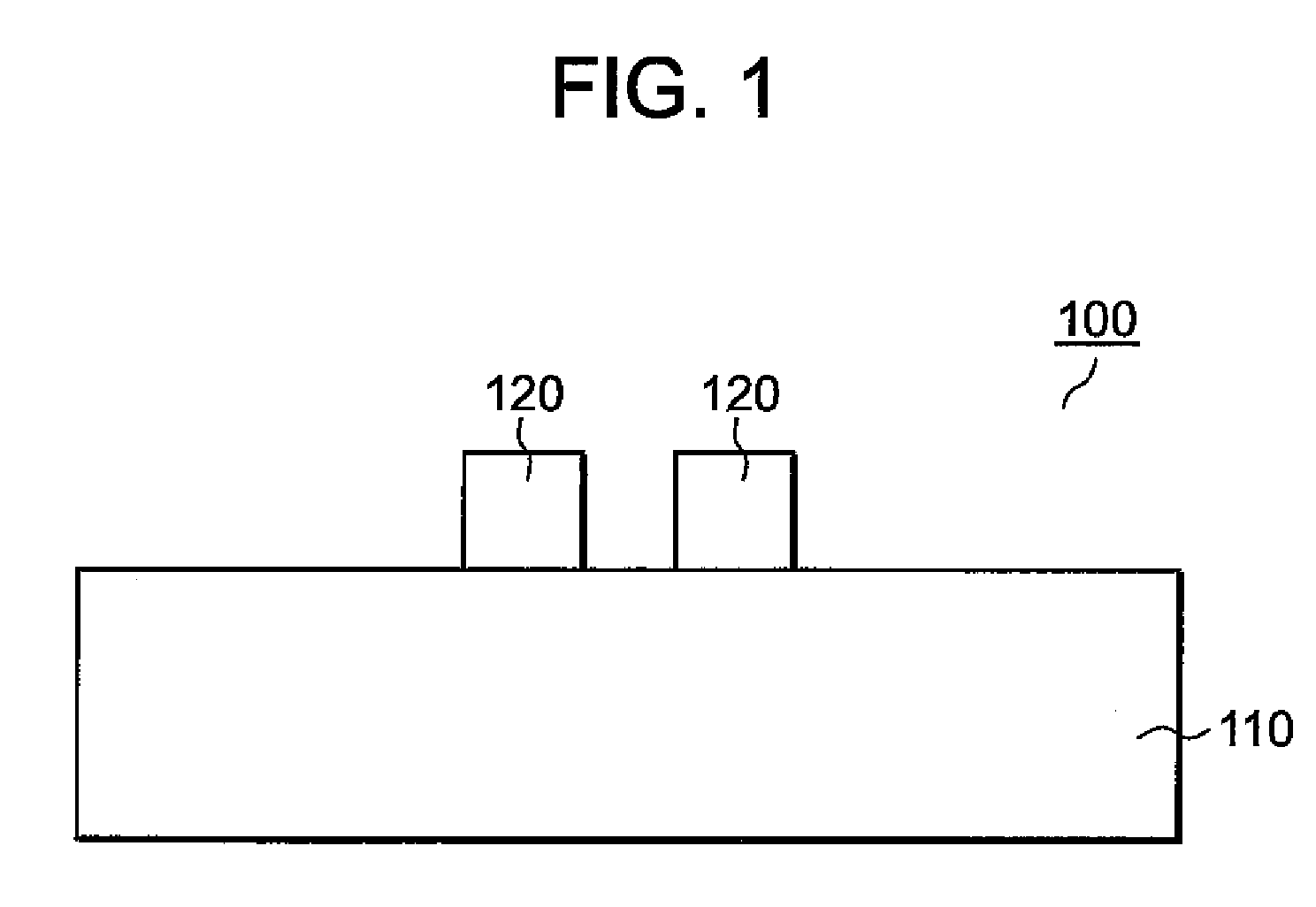
[0037]A preferred embodiment of an optical integrated circuit according to the present invention will be explained using FIGS. 1 through 5.

[0038]FIG. 1 is a sectional view conceptually showing an optical waveguide structure of the optical integrated circuit according to the present embodiment.

[0039]As shown in FIG. 1, an optical waveguide 100 according to the present embodiment includes a lower clad 110 and cores 120.

[0040]The lower clad 110 is configured by a sapphire substrate. Here, a refractive index of sapphire is 1.75 in the case of light having a light wavelength of 1550 nm. The thickness of the sapphire substrate ranges from 330 μm to 460 μm, for example.

[0041]Each of the cores 120 is comprised of a silicon film formed directly on the lower clad 110. Here, a refractive index of silicon is 3.48 in the case of a light wavelength of 1550 nm. A sectional shape of each core is rectangular and its dimensions, e.g., the thickness thereof is about 0.22 μm and the width thereof is ab...

second preferred embodiment

[0060]A second preferred embodiment of an opto-electronic integrated circuit according to the present invention will be explained using FIGS. 6 through 13.

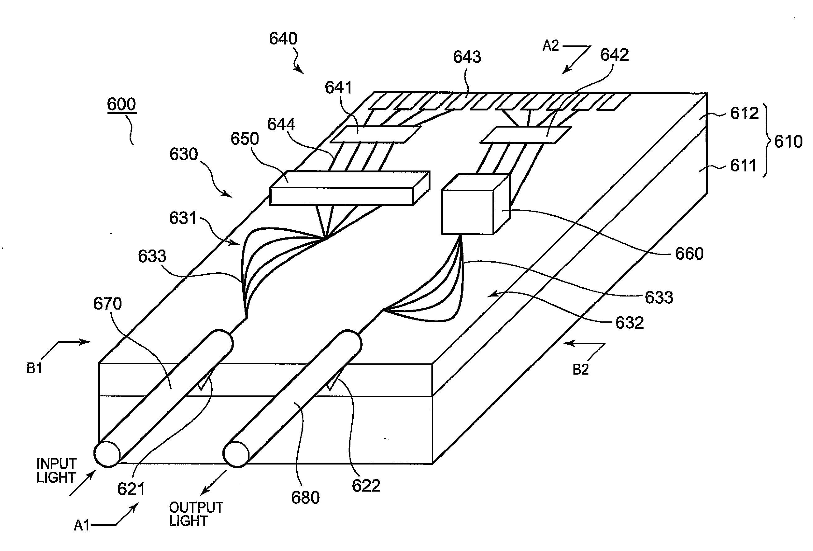
[0061]FIG. 6 is a conceptual view showing an overall configuration of the opto-electronic integrated circuit according to the present embodiment.

[0062]As shown in FIG. 6, the opto-electronic integrated circuit 600 according to the present embodiment includes an SOS substrate 610, an optical integrated circuit 630, an electronic integrated circuit 640, a photodiode array 650 and a laser diode array 660. The opto-electronic integrated circuit 600 is connected to an input optical fiber 670 and an output optical fiber 680.

[0063]The SOS substrate 610 has a sapphire substrate 611 and a silicon film 612. The sapphire substrate 611 is used as a substrate for forming the electronic integrated circuit 640 and also used as a lower clad of each optical waveguide that constitutes the optical integrated circuit 630 in a manner similar to the fi...


PUM


Abstract

In the opto-electronic integrated circuit, an optical waveguide in which a sapphire substrate for an SOS substrate is formed as a lower clad and a silicon film is formed as a core, an electronic integrated circuit formed in the silicon film, and grooves for fixing optical fibers are formed monolithically. Further, a photodiode array and a laser diode array are mounted on a hybrid basis. Since the lower clad of the optical waveguide is used as the sapphire substrate and the core is used as the silicon film, a difference in refractive index can be made large sufficiently, thus resulting in thinning of the silicon film. It is therefore possible to shorten the time required to process the core and the like. Further, since the electronic integrated circuit is formed on the sapphire substrate, the high-frequency characteristics are enhanced.

Description

BACKGROUND OF THE INVENTION[0001]The present invention relates to an optical integrated circuit using a circuit configured by an optical waveguide, an opto-electronic integrated circuit with the optical integrated circuit mounted thereto, and a method for manufacturing these.[0002]As a device using an optical waveguide circuit, there is known, for example, an opto-electronic integrated circuit. The opto-electronic integrated circuit is of a circuit in which an optical integrated circuit and a semiconductor integrated circuit are provided on the same substrate.[0003]In the optical integrated circuit, a planar lightwave circuit (PLC) is used in many cases. The planar lightwave circuit is of a circuit which realizes various functions such as light-signal multiplexing and demultiplexing and the like using an optical waveguide formed on a substrate. A configuration of the optical waveguide used in the planar lightwave circuit has been disclosed in, for example, the following non-patent d...

Claims


Application Information

Patent Timeline
IPC IPC(8): G02B6/12
CPCG02B6/12004G02B6/136G02B6/122
Inventor ARAKAWA, TOMIYUKI
Owner NEOPHOTONICS SEMICON GK
Why Eureka
Try Eureka