

Imaging Detector
a radiation detector and imaging technology, applied in the field of imaging radiation detectors, can solve the problems of material problems, problems and failure of radiation detectors, damage to read-out chips, etc., and achieve the effects of improving sensing efficiency, reducing material waste, and improving detection efficiency
- Summary
- Abstract
- Description
- Claims
- Application Information
AI Technical Summary
Benefits of technology
Problems solved by technology
Method used
Image

Examples
second embodiment
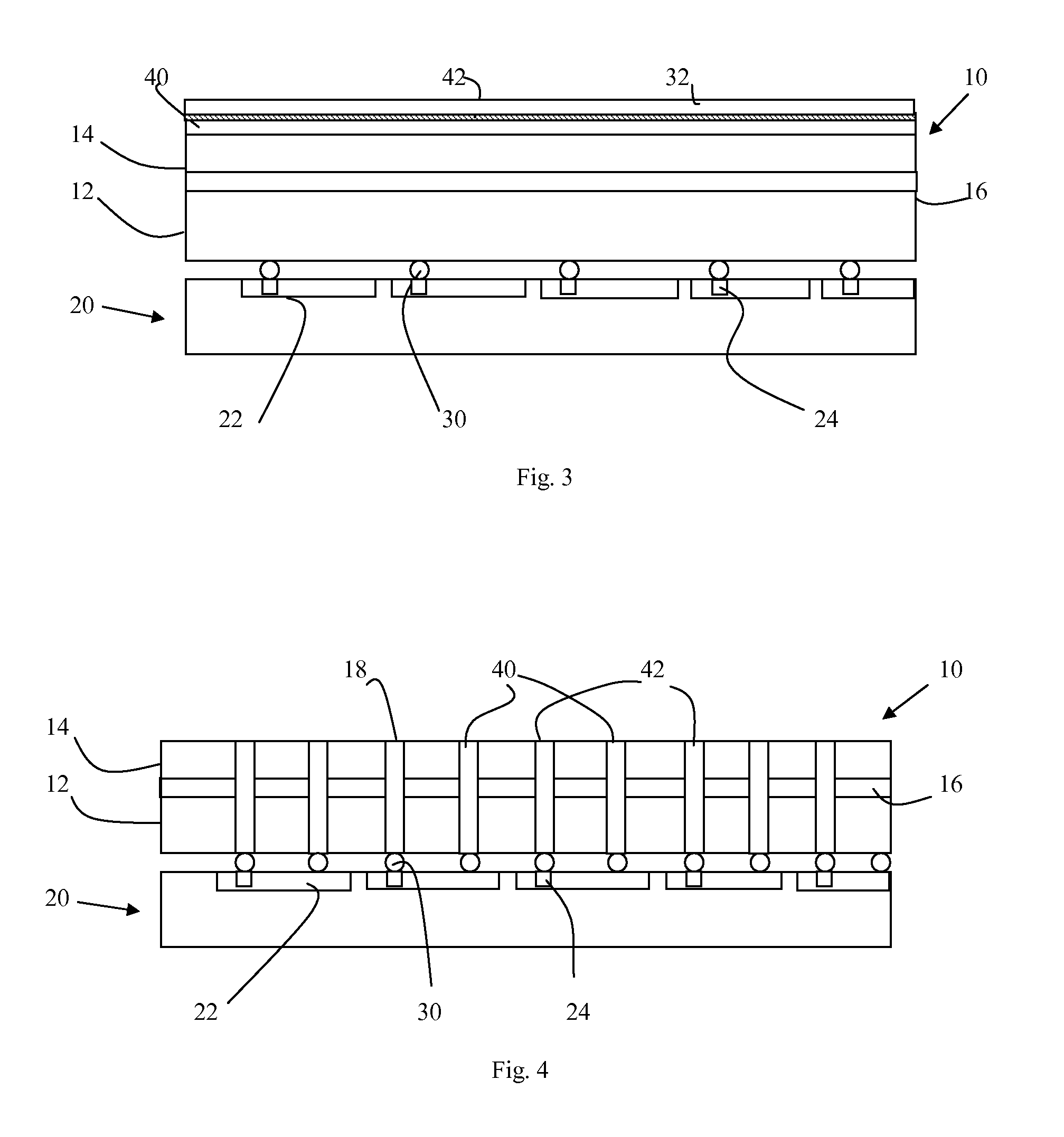
[0061]FIG. 3 illustrates a In particular, an end cap 40 of Si / SiO2 combined with a GeSi graded buffer layer having a thickness smaller than 1 μm up to 10 μm is added on top of the Ge layer 14.
[0062]The reason for the end cap is to allow the sensor 10 to be processed as if it were a Si chip, and not a chip with Ge. In order to operate the sensor 10, a voltage needs to be applied across the chip (vertically in the Figures) which means attaching an ohmic contact to the front of the chip and ohmically contacting the bump bonds 30 to the rear of the chip.
[0063]A lot of technical effort has gone into making ohmic contacts to Ge by a number of groups. Although these efforts have met with some success, and it is possible to make ohmic contacts to Ge, it is very difficult technology and not widely available or practised.
[0064]In contrast, in the arrangement of FIG. 3, by forming a thin Si capping layer on the top a top ohmic contact can be made to the Si using technology that is much better...
third embodiment
[0066]In a third embodiment, illustrated in FIG. 4, the possible impact of the interface potential on electron collection is dealt with in a different way. In particular, rods 18 are provided extending through both the first and second sensing material layers, the rods accordingly extending substantially perpendicular to the plane of the sensor 10. The rods 18 are divided into anode rods 40 and cathode rods 42, alternating across the sensor 10. The rods may be arranged in an array over the surface of the sensor. Each of the rods 18 is connected to the read-out chip, anode rod 40 is connected to a respective photon counting detector 22, and the cathode rods 42 to bias circuitry 24.
[0067]Such rods 18 can be made by machining through holes through the sensor 10 and filling the through holes with a suitable conductor such as metal.
[0068]Bias is provided between the cathode rods 42 and the anode rods 40, providing a lateral bias. In this approach, an electron cloud excited by the X-rays ...
PUM
 Abstract
Description
Claims
Application Information