Mixer circuits for second order intercept point calibration
a mixing circuit and intercept point technology, applied in the field of radio frequency receivers, can solve problems such as the leakage of transmitter signals into the receiver's receive path, the inability to accurately calibrate the intercept point, and the inability to accurately detect the signal transmitted by the transmitter
- Summary
- Abstract
- Description
- Claims
- Application Information
AI Technical Summary
Problems solved by technology
Method used
Image
Examples
first embodiment
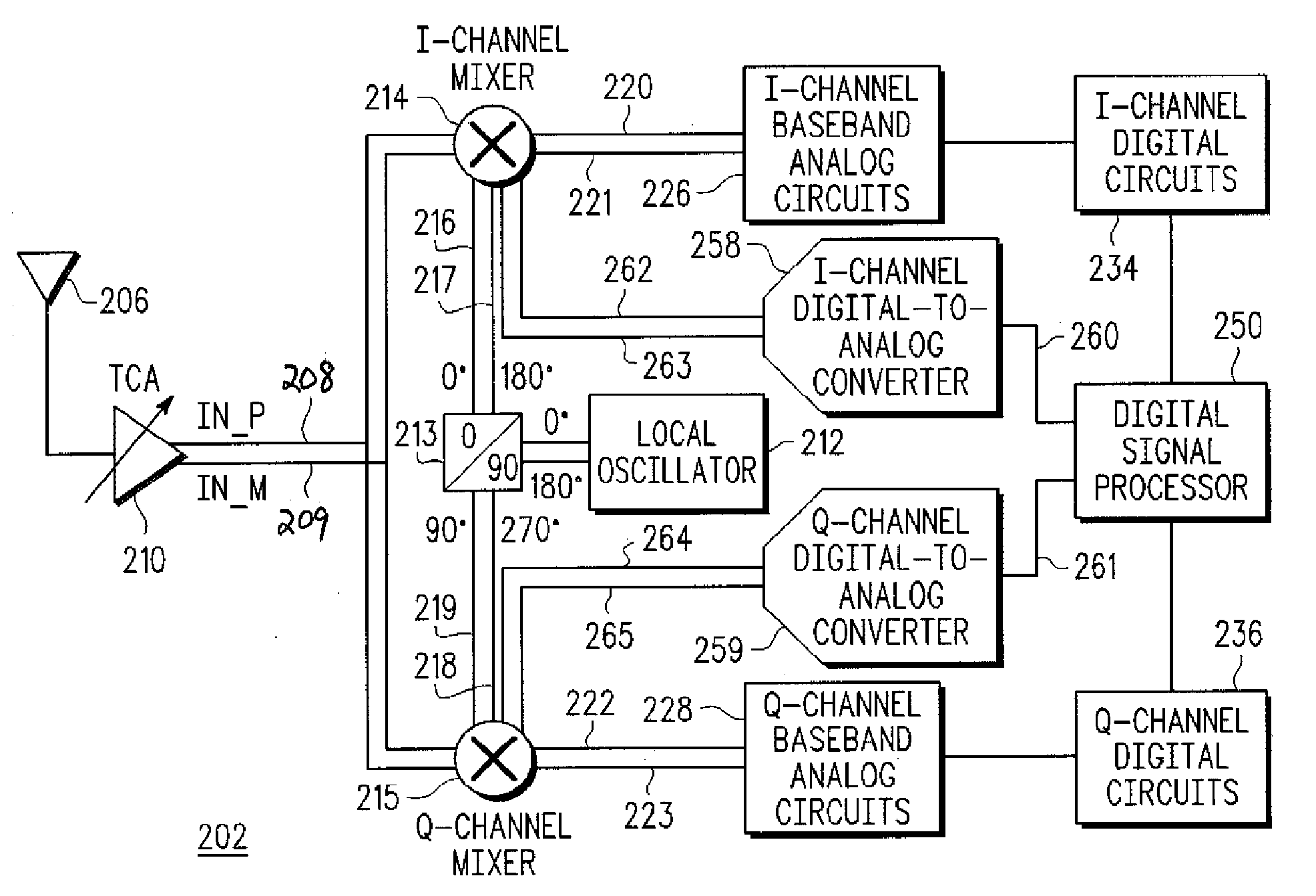
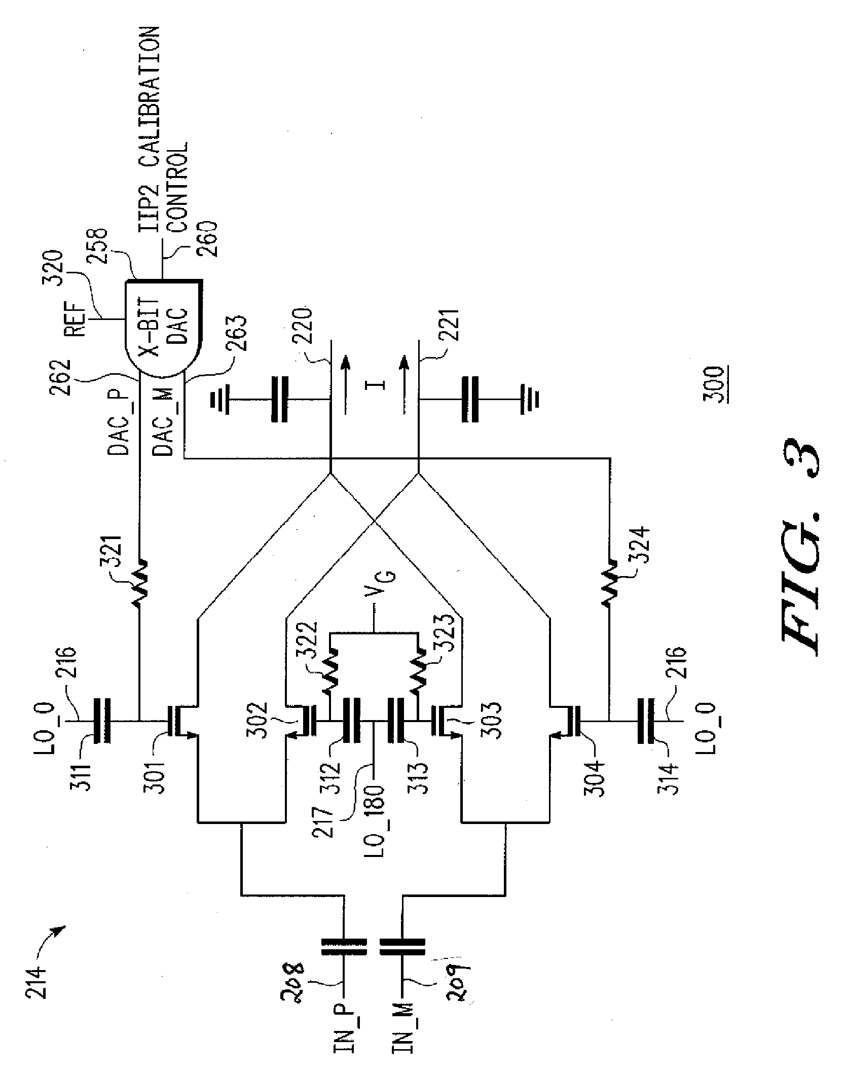
[0025]FIG. 3 is a schematic of a circuit 300 for the mixer 214. The circuit 300 illustrates a passive double balanced mixer comprising devices 301, 302, 303 and 304. The term “device” as used in this context means an active amplifying or switching device such as a transistor. In exemplary embodiments, the transistor is a CMOS transistor that includes gate, source and drain terminals. The term “passive” as used in this context, means that the mixer performs no amplification.
[0026]The circuit 300 includes an IN_P input node and an IN_M input node for receiving differential input signals IN_P 208 and IN_M 209, respectively, and two output nodes 220 and 221 for outputting differential output currents. The circuit also includes two balanced differential pairs. A first balanced differential pair includes first device 301 and second device 302 that have their sources coupled to the IN_P input node and their drains coupled to opposite output nodes. The drain of first device 301 is coupled t...
second embodiment
[0035]FIG. 4 is a schematic for a circuit 400 of the mixer 214. The circuit 400 illustrates a passive double balanced mixer comprising devices 301, 302, 303 and 304, wherein the IIP2 correction is introduced at the gate of device 301 and the gate of device 304, where the LO—0 signal and the LO—90 signal are injected. The circuit 400 includes a center tap 414 of resistors 415 and 416 across the output of the IP2 control DAC 258, which is used to provide the common-mode voltage that is applied to the gate of the devices 302 and 303 where the LO—180 signal is injected. Generating the gate bias voltage VG in this fashion tends to eliminate any common-mode offset caused by the IP2 control DAC 258. Advantageously, there is no temperature delta for the IP2 control DAC 258 because as R moves, I moves, and V stays the same.
[0036]In circuit 400, the bias voltage at the gates of devices 301 and 304 is the common-mode voltage plus the value of the IIP2 correction voltage, where the IIP2 correct...
third embodiment
[0037]FIG. 5 is a schematic for a circuit 500 of the mixer 214. The circuit 500 illustrates a passive double balanced mixer comprising devices 301, 302, 303 and 304, wherein the IIP2 correction is introduced at the gate of device 302 and at the gate of device 303, where the LO—180 signal is injected. In FIG. 5, the bias voltage at the gates of devices 302 and 303 are compensated to correct for IIP2 imbalance, as determined by the DSP 250. In FIG. 5, the bias voltage at the gates of devices 301 and 304 are uncompensated. The circuit 500 includes a center tap 414 of resistors 415 and 416 across the output of the IP2 control DAC 258, which is used to provide the bias voltage VG at the gate of the devices 301 and 304 where the LO—0 signal is injected. Alternatively, the circuit 500 does not include the center tap 414 of resistors 415 and 416 across the output of the IP2 control DAC 258, and, instead, uses the approach used in circuit 300 for providing the bias voltage VG at the gate of ...
PUM
 Abstract
Description
Claims
Application Information


