Solar cell and method for producing the same

Inactive Publication Date: 2009-08-20
SHOWA DENKO KK
View PDF4 Cites 21 Cited by
  • Summary
  • Abstract
  • Description
  • Claims
  • Application Information

AI Technical Summary

Benefits of technology

[0025]The object of the present invention is to provide a solar cell which can solve the problems, is in

Problems solved by technology

Energy consumption is rapidly increasing worldwide.
Thereby, a problem occurs in that silicon cannot be supplied to the photovoltaic market regularly due to an increase in demand for silicon in the semiconductor industry.
Specifically, although the demand for a polycrystalline silicon type solar cell, which is the most commonly used product at the present time, is rapidly increasing, the crystalline silicon material is not presently produced according to needs, and therefore the resulting supply is an increasing concern.
However, in order to increase the market for such a thin film type photovoltaic generation system, there are serious problems to be solved, such as insufficient light conversion efficiency, and the high production costs.
However, the production cost is considerably higher than that of the silicon-based solar cells.
However, the production methods and properties of such mu

Method used


Image

  • Solar cell and method for producing the same
  • Solar cell and method for producing the same
  • Solar cell and method for producing the same

Examples


example 1

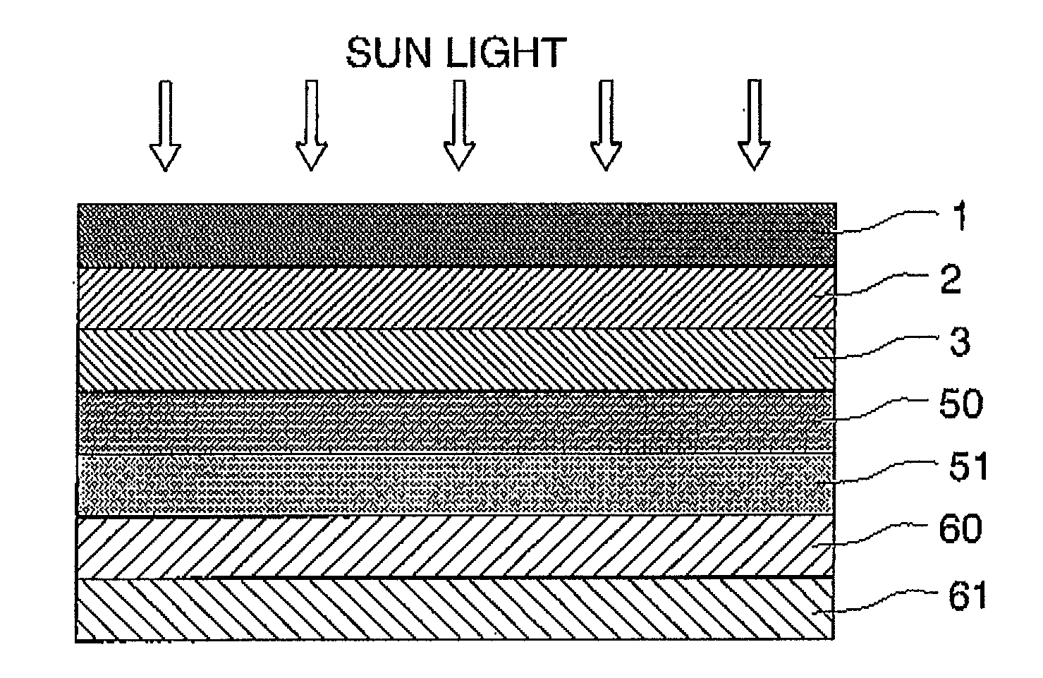
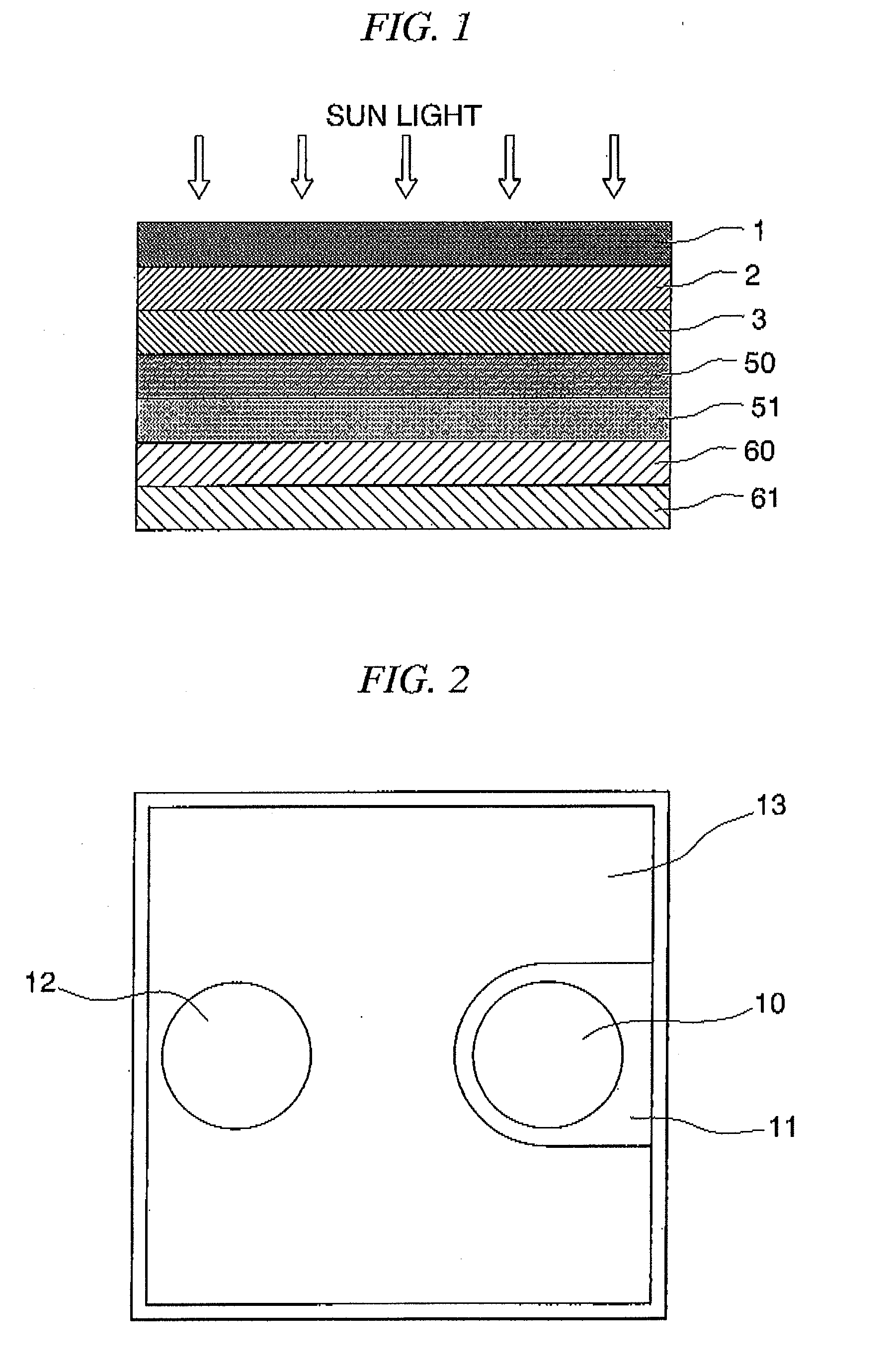
[0198]In Example 1, the solar cell including the laminate shown in FIG. 1 was produced.

[0199]First of all, the AlN buffer layer 2 having a thickness of 30 nm, and the undoped GaN base layer 3 having a thickness of 0.1 μm were layered on the quartz glass substrate 1. The used quartz glass is a commercially available optical material, and has a square size of 30 cm.

[0200]Specifically, the AlN buffer layer 2 was layered on the substrate 1 by hitting an Al target with argon plasma to beat out Al atoms, and making the Al atoms react with nitrogen, while introducing a mixed gas containing argon and nitrogen into a chamber and using nitrogen plasmas, which were obtained by applying an electrical field.

[0201]In a similar way to the AlN buffer layer 2, the undoped GaN base layer 3 was layered on the AlN buffer layer 2 by hitting a Ga target with argon plasmas to beat out Ga atoms, and making the Ga atoms react with nitrogen, while introducing a mixed gas containing argon and nitrogen into th...

example 2

[0216]The laminate shown in FIG. 1 was produced by a method which is different from the method in Example 1.

[0217]The AlN buffer layer 2 having a thickness of 30 nm was formed on the quartz substrate 1 by the RF magnetron sputtering method. Then, the substrate was removed from the sputtering device, and subjected a thermal treatment in an annealing furnace at 1,100° C. for 10 minutes under nitrogen atmosphere. After that, the substrate was introduced into the MOCVD furnace, and the p-type GaN layer 51, which was doped with Mg, was formed so as to prepare the laminate obtained in Example 1.

[0218]During the MOCVD method, common temperature, pressure, gas used, etc., were adopted.

[0219]The carrier concentration of the n-type GaN layer 50 and the p-type GaN layer 51 was about 2×10¹⁸ atoms / cm3.

[0220]Then, the solar cell element was obtained using the obtained laminate, in a similar way to Example 1. The obtained solar cell element was divided into squares in 1 cm×1 cm. The electrodes wer...

example 3

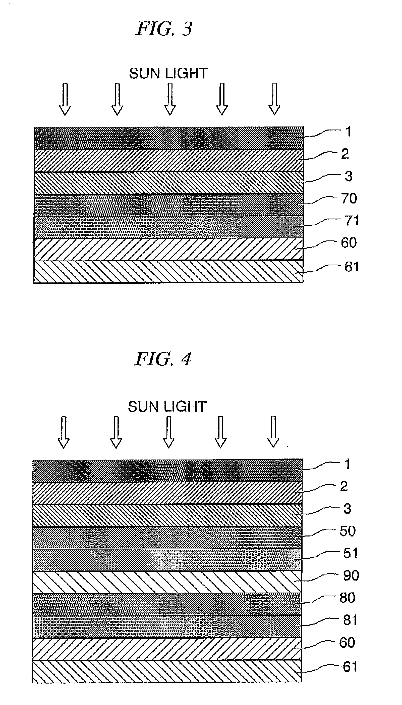
[0221]In Example 3, the solar cell including the laminate shown in FIG. 3 was produced.

[0222]First of all, an AlN buffer layer 2 having a thickness of 30 nm was formed on the quartz substrate 1 by the RF magnetron sputtering method. Then, the substrate was removed from the sputtering device, and subjected a thermal treatment in an annealing furnace at 1,100° C. for 10 minutes under nitrogen atmosphere. After that, the substrate was introduced into the MOCVD furnace. Then, the laminate, which includes the undoped GaN layer 3 having thickness of 6 μm, the n-type Inx1Ga1-x1N layer 70 (X1=0.09) having a thickness of 0.1 nm, and the p-type Inx1Ga1-x1N layer 71 (X1=0.09) having a thickness of 0.2 μm, was formed on the AlN buffer layer 2.

[0223]The carrier concentration of the n-type Inx1Ga1-x1N layer 70 and the p-type Inx1Ga1-x1N layer 71 was about 3×10¹⁸ atoms / cm3.

[0224]Then, the solar cell element was obtained using the obtained laminate, in a similar way to Example 1. The obtained solar...


PUM


Abstract

The object of the present invention is to provide a solar cell which is industrially beneficial and has high light conversion efficiency; and a method for producing a solar cell; and the present invention provides a solar cell comprising a substrate, a power generation layer for converting received light into electrical power, a translucent electrode, and another electrode, when light travels through each member from a first surface thereof, a surface opposite to the first surface is defined as a second surface, the power generation layer is formed at a second surface side of the substrate, the translucent electrode is formed on one surface of the power generation layer, and another electrode is formed on the other surface of the power generation layer, wherein the translucent electrode comprises hexagonal In2O3 crystal.

Description

BACKGROUND OF THE INVENTION[0001]1. Field of the Invention[0002]The present invention relates to a solar cell and a method for producing a solar cell. Specifically, the present invention relates to a solar cell having a laminate structure including a group III nitride semiconductor (this is also called “a group III nitride compound semiconductor”), which has excellent mass productivity and excellent properties as a solar cell, and also a method therefor.[0003]Priority is claimed on Japanese Patent Application, No. 2008-038007, filed on Feb. 19, 2008, the contents of which are incorporated herein by reference in their entirety.[0004]2. Description of the Related Art[0005]Technology related to photovoltaic generation has been in development for about thirty years. Energy consumption is rapidly increasing worldwide. In contrast, although some countries did not agree, a decrease in emission of global greenhouse gases was established worldwide under the Kyoto Protocol. Thereby, natural e...

Claims


Application Information

Patent Timeline
IPC IPC(8): H01L31/00H01L21/306
CPCH01L31/022466H01L31/0687H01L31/0693Y02E10/544H01L31/186H01L31/1884H01L31/1852Y02P70/50
Inventor IKENOUE, YOSHIAKIFUKUNAGA, NAOKISHINOHARA, HIRONAOMIKI, HISAYUKIHANAWA, KENZOKAJI, HIROAKIYOKOUCHI, HITOSHIKONTA, RYOKO
Owner SHOWA DENKO KK
Why Eureka
Try Eureka