Trench mosfet with double epitaxial structure

a technology of mosfet and mosfet plate, which is applied in the direction of semiconductor devices, electrical apparatus, transistors, etc., can solve the problems of device design facing another technical difficulty, device may not support the requirement of breakdown voltage, and further technical difficulties of device implementation, so as to reduce device resistance and low epitaxial resistivity

Active Publication Date: 2009-08-20
FORCE MOS TECH CO LTD
View PDF19 Cites 16 Cited by
  • Summary
  • Abstract
  • Description
  • Claims
  • Application Information

AI Technical Summary

Benefits of technology

[0008]It is therefore an aspect of the present invention to provide a new and improved semiconductor power device by forming a thick oxide layer at the bottom portions of a gate with a substrate provided with double epitaxial layer structure. The double epitaxial layer has a dopant concentration to provide an epitaxial resistivity that is higher near the trench bottom corners for preventing an early breakdown and a low epitaxial resistivity above the trench bottom to provide a reduced device resistance such that the difficulties and limitations of the above-discussed prior art may be overcome.

Problems solved by technology

However, a thicker oxide layer formed at the trench bottom may also cause further technical difficulties and limitations of device implementations.
Since the epitaxial layer has a resistivity that is significantly dropped in order to satisfy a design target of further reducing the Rds, the device designers now confront another technical difficulty.
With the reduction of the epitaxial resistivity, the device may not support the requirement that the breakdown voltage due to the fact that an early breakdown can occurs at the trench bottom corners.
A degradation of the breakdown voltage is therefore becoming a design and operation limitation.
However, as discussed above, when the resistivity of the epitaxial layer is decreased to provide a low Rds, the trench field plate may not support the breakdown voltage.
Additional disclosures of similar technologies are also published by M. A. Gajda et al “Industrialisation of Resurf Stepped Oxide Technology for power Transistors” (Proceedings of the 18th International Symposium on Power Semiconductor Device and ICs Jun. 4-8 2006 ISPD 2006) However, the trenched filed plate termination may not support the targeted breakdown voltage due to the lower epitaxial resistivity than the conventional devices.
Furthermore, early breakdown can often occur at the trench bottom corners that limit the applications of the device.

Method used


Image

  • Trench mosfet with double epitaxial structure
  • Trench mosfet with double epitaxial structure
  • Trench mosfet with double epitaxial structure

Examples


Embodiment Construction

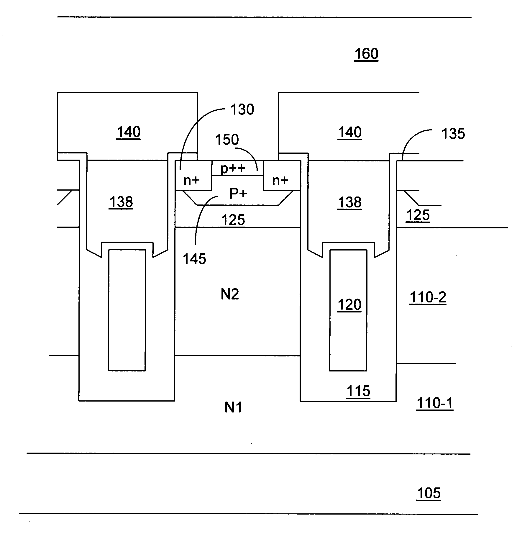
[0016]Referring to FIG. 2 for a side cross sectional view of a MOSFET device 100 formed on a N+ substrate 105 supporting a first and second N-epitaxial layer 110-1 and 110-2 having a N-dopant concentration to provide resistivity represented by N1 and N2 respectively. The resistivity N1 is greater than resistivity N2, i.e., N1>N2. The MOSFET device further includes a plurality of trenched polysilicon gates 120. Each of these trenched gates includes a top gate portion 120-T and a bottom portion 120-B wherein the top portion 120-B and the bottom portion 120-T are formed with single polysilicon deposition processes as will be further described below. At the bottom portion of the trenched gate, a gate oxide layer 115-B with a greater thickness surrounds and insulates the gate 120-B. In the top portion of the gates 120-T, a gate oxide layer 115-T has a normal and thinner layer thickness surrounds and insulates the top portion of the gate 120-T. The bottom thick gate oxide 115-B is formed ...


PUM


Abstract

A trenched semiconductor power device includes a plurality of trenched gates surrounded by source regions near a top surface of a semiconductor substrate encompassed in body regions. The trenched semiconductor power device further includes a first epitaxial layer above heavily doped substrate and beyond the trench bottom and a second epitaxial layer above said first epitaxial layer wherein a resistivity N1 of said first epitaxial layer is greater than a resistivity N2 of said second epitaxial layer represented by a functional relationship of N1>N2. In an exemplary embodiment, each of the trenched gates include an upper gate portion and lower gate portion formed with single polysilicon deposition processes wherein the lower gate portion is surrounded with a lower gate insulation layer having a greater thickness than an upper gate insulation layer surrounding the upper gate portion.

Description

BACKGROUND OF THE INVENTION[0001]1. Field of the Invention[0002]The invention relates generally to the device configuration and manufacturing methods for fabricating the semiconductor power devices. More particularly, this invention relates to an improved and novel manufacturing process and device configuration for providing the MOSFET device with double epitaxial layers to improve the breakdown voltage while reducing the on-resistance of the semiconductor power device.[0003]2. Description of the Related Art[0004]In order to increase the switching speed of a semiconductor power device, it is desirable to reduce the electric charges between the gate and drain such that a reduction of a gate to drain capacitance Crss can be reduced. A thick oxide formed at the trench bottom of the trench gate is frequently implemented to reduce the gate to drain capacitance. However, a thicker oxide layer formed at the trench bottom may also cause further technical difficulties and limitations of devi...

Claims


Application Information

Patent Timeline
Patent Type & Authority Applications(United States)
IPC IPC(8): H01L29/78H01L21/336
CPCH01L29/0878H01L29/7813H01L29/66734H01L29/42368H01L29/086
Inventor HSHIEH, FWU-IUAN
Owner FORCE MOS TECH CO LTD
Why Eureka
Try Eureka