P-Type Amorphous GaNAs Alloy as Low Resistant Ohmic Contact to P-Type Group III-Nitride Semiconductors

a ganas alloy and ohmic contact technology, applied in the field of amorphous ganas film do, can solve the problems of barrier impeding charge transport across the interface, forming a depletion region, and not meeting the conduction requirement of platinum with the highest work function of 5.4 ev, so as to reduce the resistance of the device

Inactive Publication Date: 2013-05-23
RGT UNIV OF CALIFORNIA
View PDF3 Cites 2 Cited by
  • Summary
  • Abstract
  • Description
  • Claims
  • Application Information

AI Technical Summary

Benefits of technology

[0013]As an ohmic contact layer, it is best to keep the GaNAs:Mg layer quite thin, such as in the range of between 5 and 50 nm, and more preferably <20 nm. Further, and by way of example, when the heavily p-type doped GaNAs layer is inserted between a p-GaN layer and a high work function metal (such as platinum), the large barrier (˜2 eV) can be reduced to <1 eV between the GaNAs and the GaN, thus drastically reducing the resistance of the device. In the case of an InGaN—Si hybrid type solar cell, using the highly p-type GaNAs layer as an ohmic contact interlayer between the metal contact can essentially eliminate the ˜1.1 eV energy barrier.

Problems solved by technology

However, even platinum with the highest work function of 5.4 eV does not satisfy this conduction requirement.
In fact the majority of the metal semiconductor contacts are far from being ideal, in most instances, the Fermi energy at the metal / semiconductor interface is pinned, resulting in the formation of a depletion region and barrier impeding charge transport across the interface.
The main problem with p-type group III-nitrides, however, is that the doping (larger than 1019 / cm3) required for low resistance contacts simply cannot be achieved.
Consequently reliable low resistance ohmic contacts on p-type group III-nitrides are difficult to realize.
However, due to the complexity of the metallization scheme, good ohmic contacts to p-type GaN are not always reproducible, even using identical procedures.

Method used


Image

  • P-Type Amorphous GaNAs Alloy as Low Resistant Ohmic Contact to P-Type Group III-Nitride Semiconductors
  • P-Type Amorphous GaNAs Alloy as Low Resistant Ohmic Contact to P-Type Group III-Nitride Semiconductors
  • P-Type Amorphous GaNAs Alloy as Low Resistant Ohmic Contact to P-Type Group III-Nitride Semiconductors

Examples


Embodiment Construction

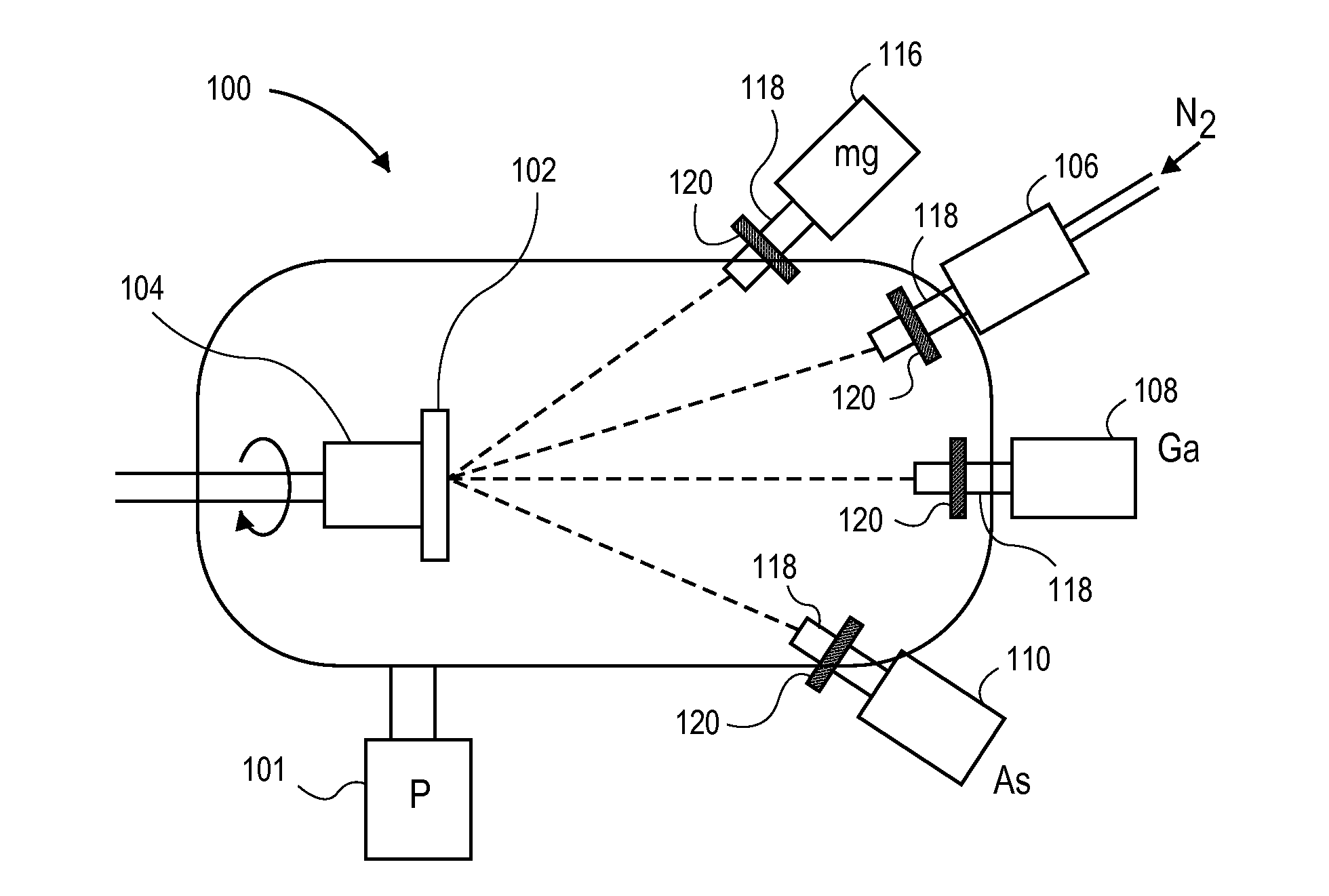
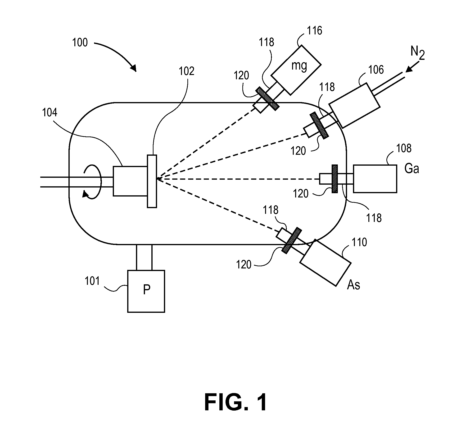
[0024]With reference to FIG. 1, a schematic of an MBE apparatus, an MBE chamber 100 is served by one or more turbo and / or cryo pumps 101 capable of achieving the necessary high vacuum conditions (e.g. 10−9 to 10−10 Torr). A substrate holder or platter 102 is provided upon which the substrate to be coated is placed. Heater 104 is provided below substrate holder 102, which heater is capable of heating the substrate to temperatures in excess of 700° C. A mechanism (not shown) can be used to rotate the heater and holder during the deposition process. The elements to be incorporated into the film alloy are provided in solid form and placed in individual crucibles (not shown) which are located in respective ovens / furnaces 108 and 110. Using heaters in these furnaces capable of heating the solids to temperatures above their sublimation and melting temperatures, the elements are vaporized to gaseous form and introduced into the deposition chamber through portals 118. The relative amounts of...


PUM

PropertyMeasurementUnit
thicknessaaaaaaaaaa
thicknessaaaaaaaaaa
thicknessaaaaaaaaaa

Abstract

A new composition of matter is described, amorphous GaN1-xAsx:Mg, wherein 0<x<1, and more preferably 0.1<x<0.8, which amorphous material is of low resistivity, and when formed as a thin, heavily doped film may be used as a low resistant p-type ohmic contact layer for a p-type group III-nitride layer in such applications as photovoltaic cells. The layer may be applied either as a conformal film or a patterned layer. In one embodiment, as a lightly doped but thicker layer, the amorphous GaN1-xAsx:Mg film can itself be used as an absorber layer in PV applications. Also described herein is a novel, low temperature method for the formation of the heavily doped amorphous GaN1-xAsx:Mg compositions of the invention in which the doping is achieved during film formation according to MBE methods.

Description

CROSS REFERENCE TO RELATED APPLICATIONS[0001]This US application claims priority to U.S. Provisional Application Ser. No. 61 / 488,036 filed May 19, 2011, which application is incorporated herein by reference as if fully set forth in their entirety.STATEMENT OF GOVERNMENTAL SUPPORT[0002]The invention described and claimed herein was made in part utilizing funds supplied by the U.S. Department of Energy under Contract No. DE-AC02-05CH1231 between the U.S. Department of Energy and the Regents of the University of California for the management and operation of the Lawrence Berkeley National Laboratory. The government has certain rights in this invention.BACKGROUND OF THE INVENTION[0003]1. Field of the Invention[0004]This invention relates generally to a novel composition of matter comprising an amorphous, p-doped GaNAs, and more particularly to an amorphous GaNAs film doped with Mg, and a method of preparation thereof, which film can serve as a low resistance ohmic contact layer in such ...

Claims


Application Information

Patent Timeline
Patent Type & Authority Applications(United States)
IPC IPC(8): H01L29/20H01L21/04
CPCH01L29/2003H01L21/04H01L21/0254H01L21/02546H01L21/28575H01L31/03048H01L31/0693Y02E10/544H01L33/325H01L33/40H01L29/452H01L31/03044H01L31/0376
Inventor YU, KIN MANWALUKIEWICZ, WLADYSLAWLEVANDER, ALEJANDRO X.NOVIKOV, SERGEI V.FOXON, C. THOMAS
Owner RGT UNIV OF CALIFORNIA
Why Eureka
Try Eureka