Planar High-Electron-Mobility Transistor

a high-electron-mobility, transistor technology, applied in the direction of semiconductor devices, basic electric elements, electrical equipment, etc., can solve the problem of not having a consensus in the industry on the way to realize normally-off gallium nitride, and achieve the effect of improving the breakdown voltage of the device, reducing the specific on resistance of the device, and reducing the size of the devi

Pending Publication Date: 2022-06-23
NANTONG SANRISE INTEGRATED CIRCUIT CO LTD
View PDF0 Cites 0 Cited by
  • Summary
  • Abstract
  • Description
  • Claims
  • Application Information

AI Technical Summary

Benefits of technology

[0043]The present application can cut off the two-dimensional electron gas by forming a trench gate and passing the bottom of the gate trench of the trench gate to a position under the two-dimensional electron gas, so that the formation of the conductive channel between the source and the drain is not controlled by the two-dimensional electron gas, but by the trench gate. The inversion layer formed by the inversion of the first semiconductor epitaxial layer through the trench gate can realize the on and off control of the conductive channel. That is, the present application can realize the control of the conductive channel of the HEMT by adopting the trench gate of the MOSFET. In this way, the planar high-electron-mobility transistor, like the MOSFET, can control the on and off of the conductive channel through the trench gate, thus facilitating the independent adjustment of the threshold voltage of the planar high-electron-mobility transistor, for example, adjusting the threshold voltage of the device by adjusting the work function of the gate conductive material layer of the trench gate, the thickness of the gate dielectric layer and the doping type and doping concentration of the first semiconductor epitaxial layer, and facilitating the realization of a normally-off planar high-electron-mobility transistor. However, the two-dimensional electron gas of the existing planar high-electron-mobility transistor is conducted and it is a normally-on device. The present application facilitates the realization of a normally-off planar high-electron-mobility transistor.
[0044]In addition, the present application can form a charge balance structure in the drift region between the trench gate and the drain metal layer, and adjust the electric field distribution in the drift region through the charge balance structure, thus conveniently obtaining the uniformly distributed electric field in the drift region, improving the breakdown voltage of the device, reducing the specific on resistance of the device while maintaining the adjustment of the breakdown voltage, reducing the size of the device, and greatly reducing the energy loss when the device is on. The present application can be applied to gallium nitride materials, give full play to the advantages of gallium nitride materials, reduce the manufacturing cost of gallium nitride devices and simplify the process flow.
[0045]The gallium nitride power device structure according to the present application can conveniently adjust the threshold voltage, so as to manufacture an enhanced transistor and make its application scope wider. Compared with the traditional high-electron-mobility transistors, under the same breakdown voltage, the specific on resistance is greatly reduced relative to the existing power device, thus greatly reducing the power loss of power semiconductor devices, saving energy, reducing emission, giving full play to the advantages of gallium nitride devices, simplifying the process flow and reducing the manufacturing cost.

Problems solved by technology

However, there is no consensus in the industry on the way to realize normally-off gallium nitride HEMTs.

Method used


Image

  • Planar High-Electron-Mobility Transistor
  • Planar High-Electron-Mobility Transistor
  • Planar High-Electron-Mobility Transistor

Examples


embodiment 1

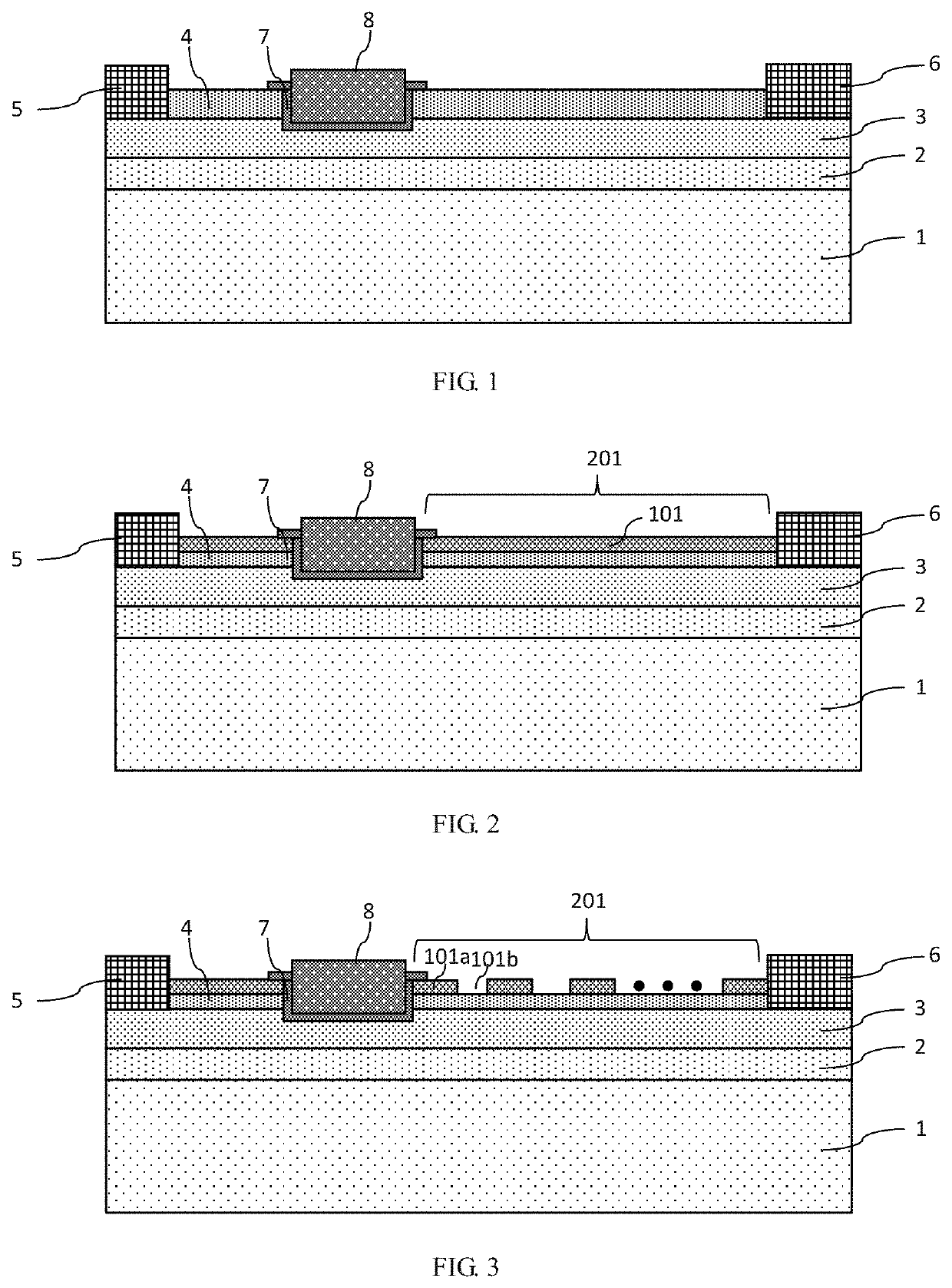
[0063 of the present application provides a planar high-electron-mobility transistor.

[0064]Referring to FIG. 2, it illustrates a schematic diagram of a structure of the planar high-electron-mobility transistor according to embodiment 1 of the present application. A device unit of the planar high-electron-mobility transistor according to embodiment 1 of the present application includes:

[0065]a first semiconductor epitaxial layer 3 and a second semiconductor epitaxial layer 4 formed on a surface of the first semiconductor epitaxial layer 3, the first semiconductor epitaxial layer 3 and the second semiconductor epitaxial layer 4 forming a first hetero-junction and forming two-dimensional electron gas at an interface of the first hetero-junction;

[0066]a trench gate including a gate trench, a gate dielectric layer 7 formed on an inner side surface of the gate trench and a gate conductive material layer 8 filled in the gate trench.

[0067]The gate trench passes through the second semiconduc...

embodiment 2

[0086 of the present application provides a planar high-electron-mobility transistor.

[0087]The planar high-electron-mobility transistor according to embodiment 2 of the present application has the following difference from the planar high-electron-mobility transistor according to embodiment 1 of the present application: the planar high-electron-mobility transistor according to embodiment 2 of the present application further includes the following features:

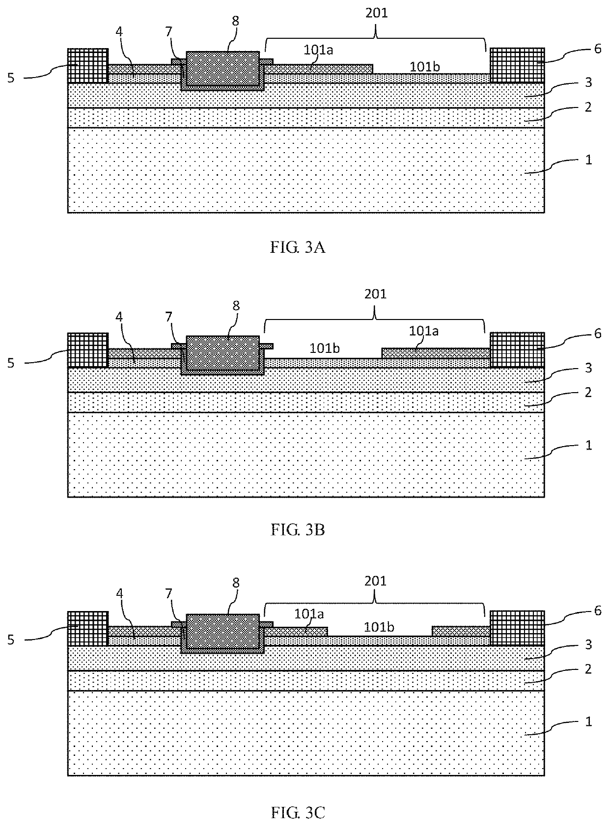
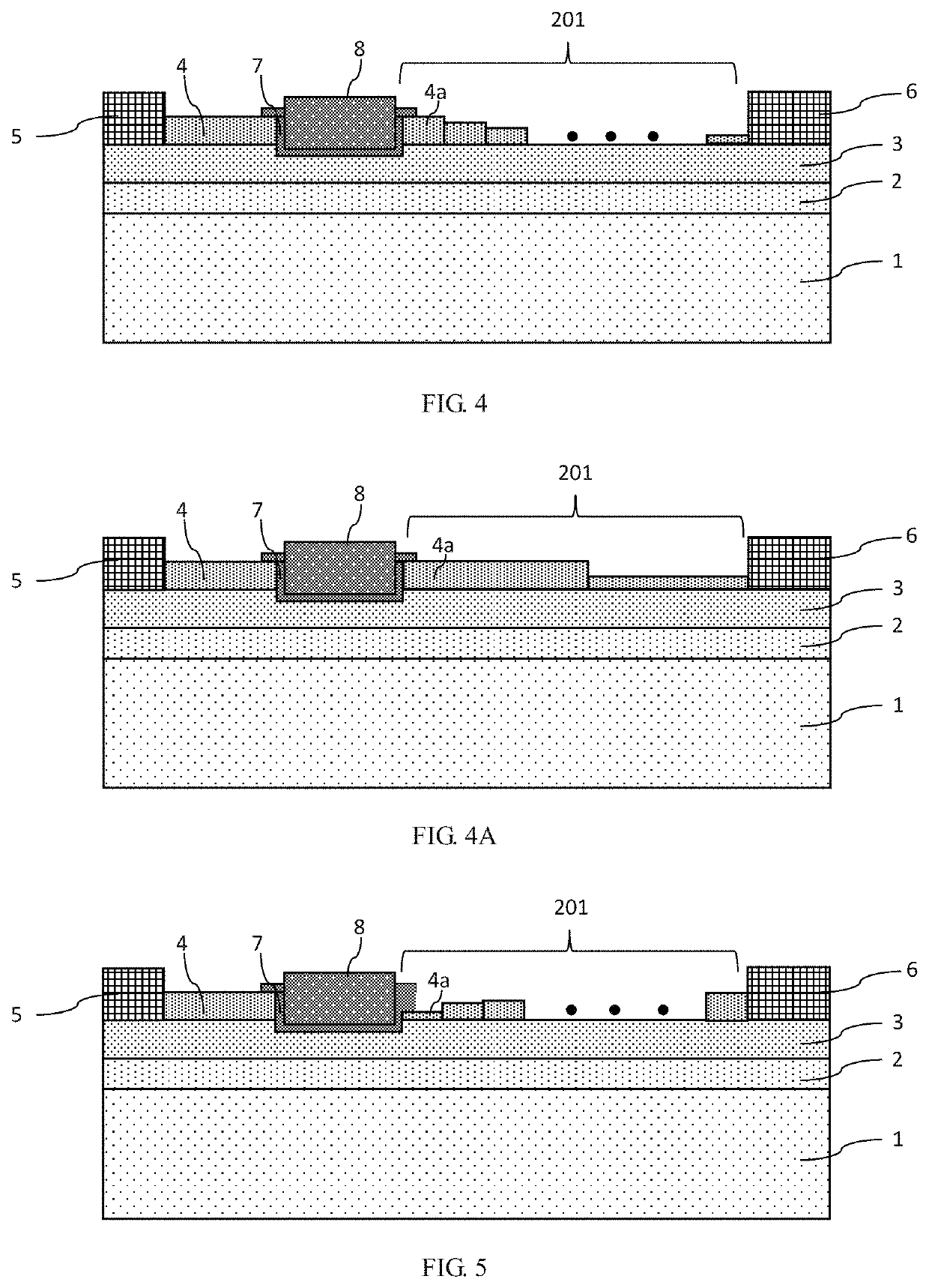
[0088]Referring to FIG. 2, it illustrates a schematic diagram of a structure of the planar high-electron-mobility transistor according to embodiment 2 of the present application. The drift region is located between the drain metal layer 6 and the second side surface of the gate trench, a charge balance structure is arranged in the drift region, and during reverse bias, the charge balance structure enables the electric field distribution in the drift region to be uniform. In FIG. 2, the transverse region corresponding to the drift r...

embodiment 3

[0096 of the present application provides a planar high-electron-mobility transistor.

[0097]The planar high-electron-mobility transistor according to embodiment 3 of the present application has the following difference from the planar high-electron-mobility transistor according to embodiment 2 of the present application: the planar high-electron-mobility transistor according to embodiment 3 of the present application further includes the following features:

[0098]Referring to FIG. 3, it illustrates a schematic diagram of a structure of the planar high-electron-mobility transistor according to embodiment 3 of the present application. On the surface of the second semiconductor epitaxial layer 4 in the drift region, the third semiconductor epitaxial layer 101 is divided into more than one third semiconductor epitaxial layer sub-segments 101a and more than one third semiconductor epitaxial layer spacer regions 101b, the third semiconductor epitaxial layer sub-segments 101a and the third s...


PUM

PropertyMeasurementUnit
threshold voltageaaaaaaaaaa
thicknessaaaaaaaaaa
breakdown electric field strengthaaaaaaaaaa

Abstract

The present application discloses a planar High-Electron-Mobility Transistor (HEMT), which includes a hetero-junction consisting of a first semiconductor epitaxial layer and a second semiconductor epitaxial layer, and two-dimensional electron gas located at an interface of the hetero-junction; a bottom surface of a gate trench of a trench gate is located at a bottom of the two-dimensional electron gas to cut off the two-dimensional electron gas; when gate-source voltage is higher than or equal to threshold voltage, an inversion layer is formed on a surface of the first semiconductor epitaxial layer covered by side surfaces and a bottom surface of a gate conductive material layer, and the source-end and drain-end two-dimensional electron gas is conducted to enable the device to be on; when the gate-source voltage is lower than the threshold voltage, the source-end and drain-end two-dimensional electron gas is cut off to enable the device to be off.

Description

CROSS-REFERENCES TO RELATED APPLICATIONS[0001]This application claims priority to Chinese Patent Application No. 202011536169.0, filed on Dec. 23, 2020, the disclosure of which is incorporated herein by reference in its entirety.TECHNICAL FIELD[0002]The present application relates to the field of semiconductor integrated circuit manufacturing, in particular to a planar High-Electron-Mobility Transistor (HEMT).BACKGROUND[0003]As a typical wide-bandgap semiconductor material, gallium nitride is often used in the manufacture of power semiconductor devices in various studies. Especially in the application of high temperature and high voltage, the gallium nitride material has more obvious advantages because of its large bandgap of 3.4 eV, high breakdown electric field strength of 3 MV / cm, high electron mobility and high thermal conductivity. So far, the mainstream gallium nitride devices still focus on the research of planar HEMTs. The manufacturing process of this kind of devices has gr...

Claims


Application Information

Patent Timeline
Patent Type & Authority Applications(United States)
IPC IPC(8): H01L29/778H01L29/423H01L29/20H01L29/205H01L29/417
CPCH01L29/7783H01L29/4236H01L29/4175H01L29/205H01L29/2003H01L29/0615H01L29/7787H01L29/66462H01L29/7786H01L29/0657
Inventor ZHOU, XIANG
Owner NANTONG SANRISE INTEGRATED CIRCUIT CO LTD
Why Eureka
Try Eureka