Semitubular metal-oxide-semiconductor field effect transistor

a metal-oxide-semiconductor and semi-tubular technology, applied in the direction of transistors, semiconductor devices, electrical equipment, etc., can solve the problems of mosfet threshold voltages which are difficult to anticipate and control, scaling of semiconductor devices, and threshold voltage and leakage current at semiconductor junctions

Inactive Publication Date: 2009-08-27
GLOBALFOUNDRIES INC
View PDF10 Cites 29 Cited by
  • Summary
  • Abstract
  • Description
  • Claims
  • Application Information

AI Technical Summary

Benefits of technology

[0009]The present invention addresses the needs described above by providing a metal-on-semiconductor fi

Problems solved by technology

As the device scale approaches nanometer ranges, further scaling of semiconductor devices faces various challenges.
Some challenges arise from the quantum mechanical nature of material properties at atomic dimensions such as gate tunneling current.
Some other challenges arise from the stochastic nature of material properties such as fluctuations in dopant concentration on a microscopic scale, and resulting spread in threshold voltage and leakage current at semiconductor junctions.
Furthermore, th

Method used


Image

  • Semitubular metal-oxide-semiconductor field effect transistor
  • Semitubular metal-oxide-semiconductor field effect transistor
  • Semitubular metal-oxide-semiconductor field effect transistor

Examples


first embodiment

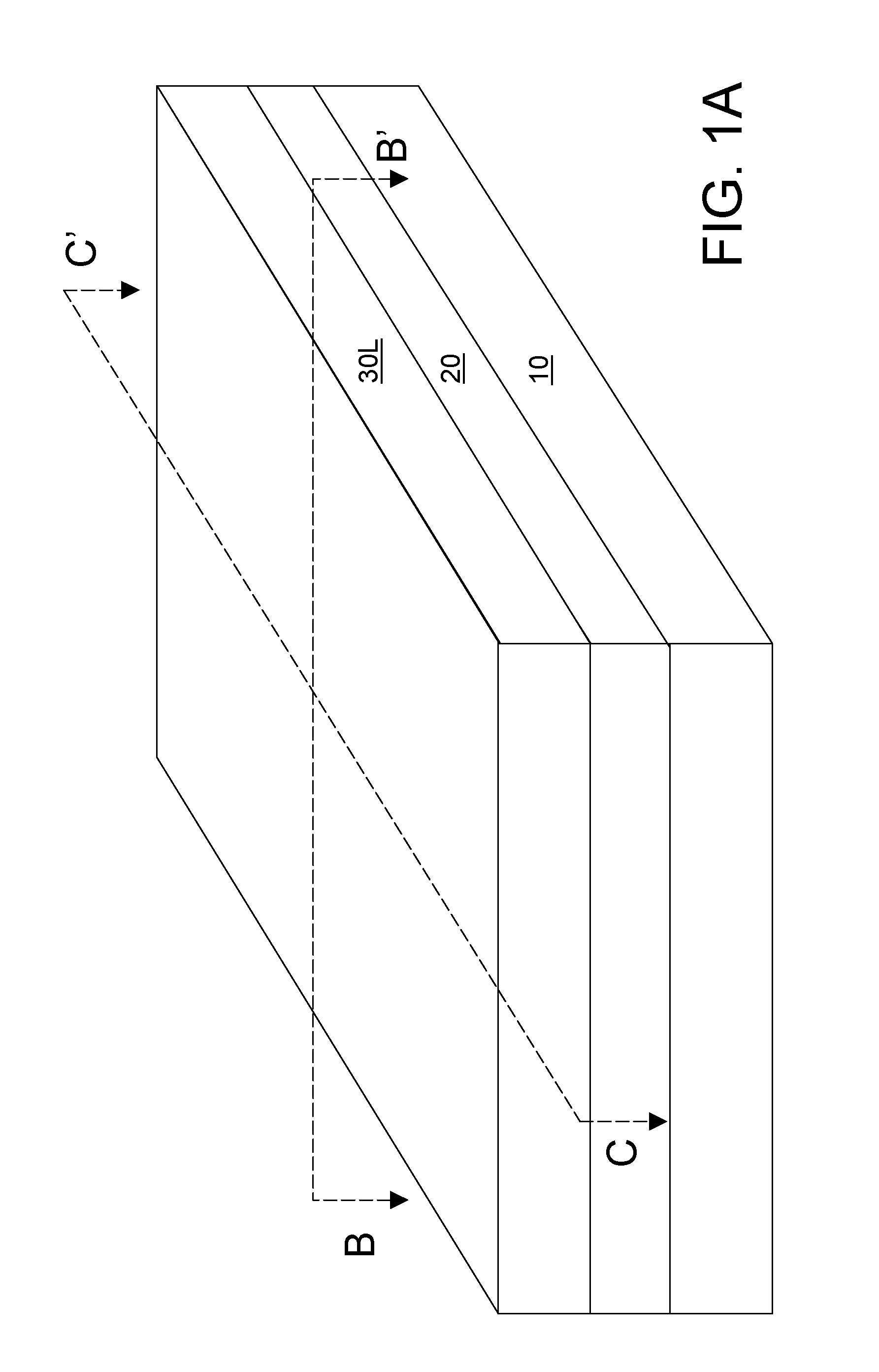
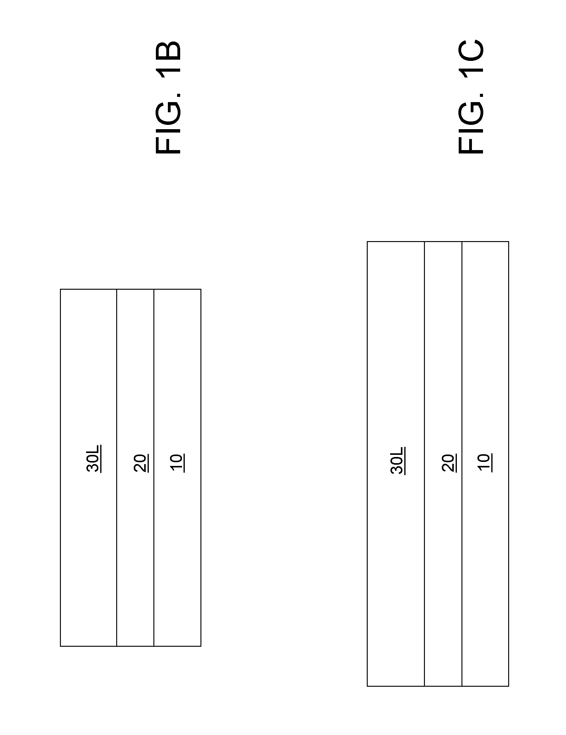
[0087]Referring to FIGS. 1A-1C, a first exemplary semiconductor structure according to the present invention is shown, which comprises a semiconductor-on-insulator substrate including a handle substrate 8, an insulator layer 20, and a top silicon layer 30L. The handle substrate 10 may comprise a semiconductor material, metallic material, or an insulator material providing structural support for the insulator layer 20 and the top silicon layer 30L. The insulator layer 20 comprises an insulator material such as a dielectric oxide or a dielectric nitride. The insulator layer 20 may comprise a crystalline material or a non-crystalline material. For example, the insulator layer 20 may comprise silicon nitride, silicon oxynitride, silicon oxide, or a ceramic material.

[0088]A top portion of the insulator layer 20 comprises a material that may withstand a porosification process to be subsequently performed. The semiconductor material may be selected from, but is not limited to, silicon, ger...

second embodiment

[0134]Referring to FIGS. 14A and 14B, a second exemplary semiconductor structure according to the present invention is derived from the first exemplary semiconductor structure of FIGS. 3A-3C by forming a silicon-germanium alloy layer 131 directly on the porous silicon portion 30′. The silicon-germanium alloy layer 131 is epitaxially deposited on exposed surfaces of the porous silicon portion 30′. To effect the deposition of the silicon-germanium alloy layer 131, the second exemplary semiconductor structure is placed in a reactor and a silicon-containing reactant gas and a germanium-containing reactant gas are flown into the reactor with a carrier gas such as H2 or He. Exemplary silicon-containing reactant gases include SiH4, SiH2Cl2, SiHCl3, SiCl4, Si2H6, etc., or a combination thereof. Exemplary germanium-containing reactant gases include GeH4, Ge2H6, etc.

[0135]In an embodiment of the present invention, the epitaxial deposition of the silicon-germanium alloy layer 131 is performed ...


PUM


Abstract

An epitaxial semiconductor layer or a stack of a silicon germanium alloy layer and an epitaxial strained silicon layer is formed on outer sidewalls of a porous silicon portion on a substrate. The porous silicon portion and any silicon germanium alloy material are removed and a semitubular epitaxial semiconductor structure in a three-walled configuration is formed. A semitubular field effect transistor comprising inner and outer gate dielectric layers, an inner gate electrode, an outer gate electrode, and source and drain regions is formed on the semitubular epitaxial semiconductor structure. The semitubular field effect transistor may operate as an SOI transistor with a tighter channel control through the inner and outer gate electrodes, or as a memory device storing electrical charges in the body region within the semitubular epitaxial semiconductor structure.

Description

FIELD OF THE INVENTION [0001]The present invention relates to a metal-oxide-semiconductor semitubular field effect transistor (MOSFET) structures and methods of manufacturing the same.BACKGROUND OF THE INVENTION [0002]Continuous scaling of silicon-based metal oxide semiconductor field effect transistors (MOSFETs) has contributed to relentless advances in semiconductor technology. As the device scale approaches nanometer ranges, further scaling of semiconductor devices faces various challenges. Some challenges arise from the quantum mechanical nature of material properties at atomic dimensions such as gate tunneling current. Some other challenges arise from the stochastic nature of material properties such as fluctuations in dopant concentration on a microscopic scale, and resulting spread in threshold voltage and leakage current at semiconductor junctions. These and other challenges in semiconductor technology have renewed interest in semiconductor devices having non-conventional ge...

Claims


Application Information

Patent Timeline
IPC IPC(8): H01L29/788H01L21/336
CPCH01L27/108H01L27/10802H01L29/7853H01L29/66795H01L29/7841H01L27/10826H10B12/20H10B12/36H10B12/00
Inventor CHENG, KANGGUOCLEVENGER, LAWRENCE A.DALTON, TIMOTHY J.HSU, LOUIS L.MANDELMAN, JACK A.
Owner GLOBALFOUNDRIES INC
Why Eureka
Try Eureka