[0044]It is an object of the invention to increase the effectiveness of the
chemical treatment and cleaning and
drying operations, and to reduce the cost of such operations. Further objects are to improve the safety of the
chemical treatment and cleaning and drying operations and to reduce the
discharge of hazardous or noxious substances from the treating and cleaning operations. It is another object to provide a device and a method for cleaning semiconductor wafers by taking
advantage of the desirable characteristic of foam, which from a volumetric standpoint consists mostly of gas and therefore delivers a reduced amount of
small particles of contaminant to the surface of the wafer. A further object is to provide an apparatus for foam-based cleaning which has an extremely simple and inexpensive construction for both processes of cleaning and drying. It is a further object to provide the apparatus of the aforementioned type to be free of mechanically
moving parts. Another object is to provide a foam-based cleaning method and apparatus that allow the use of different chemical components for foam-creating liquids, with adjustment and control of the foam parameters over a wide range.
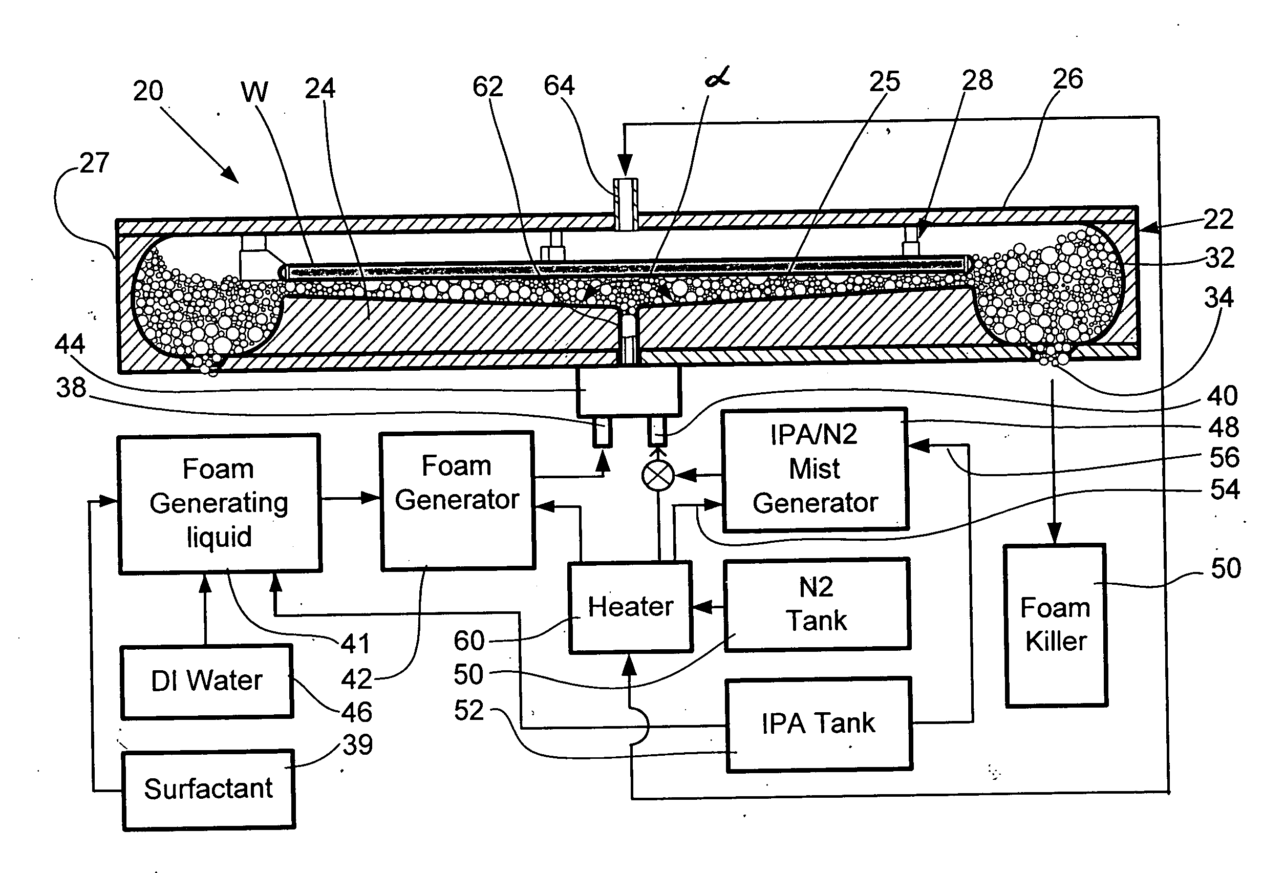
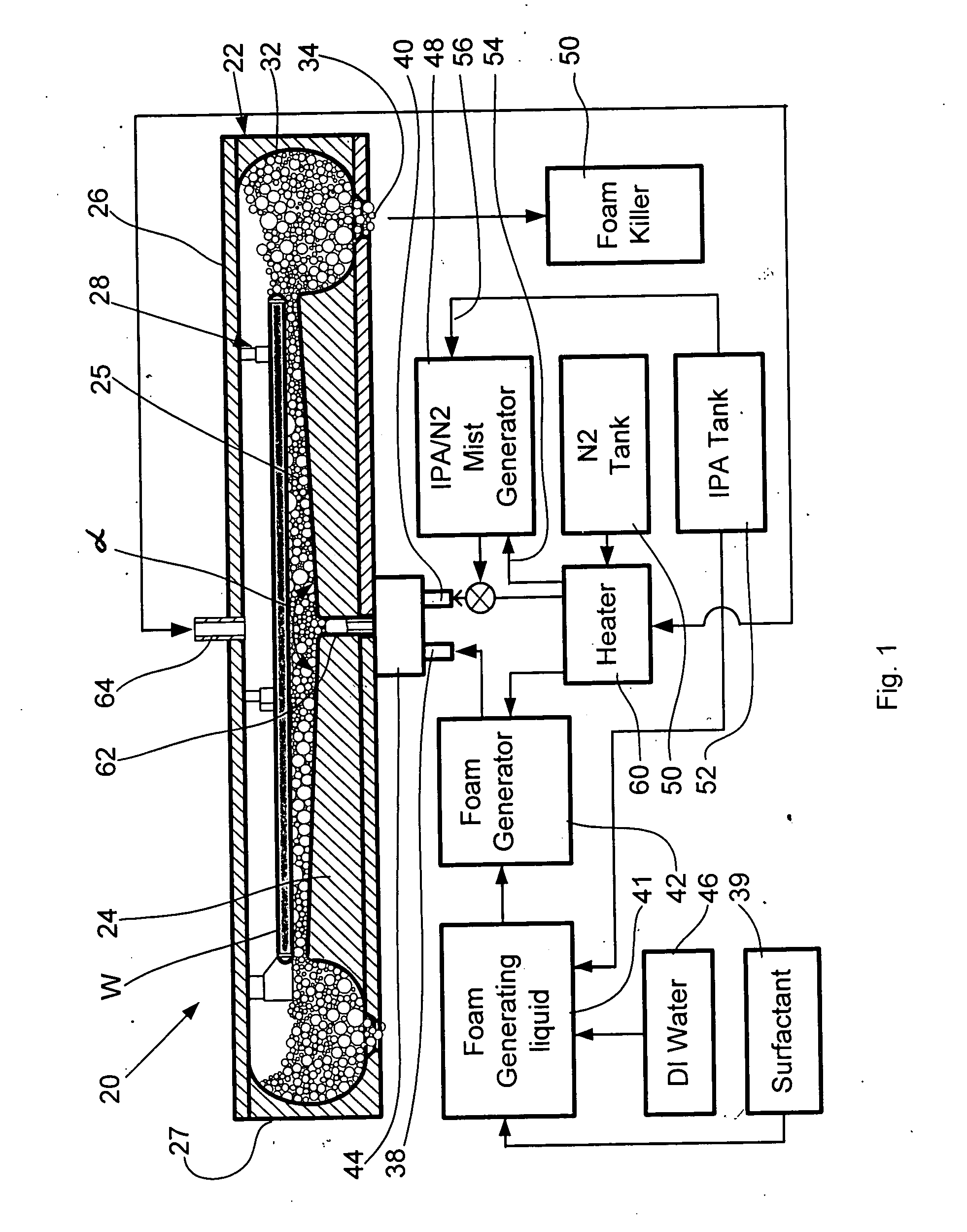
[0046]The apparatus operates as follows. The cover is disconnected from the shallow container or pivotally turned for access to the wafer-gripping mechanism, and the wafer to be treated is inserted into the gripper and clamped by moving the gripping fingers radially inward. The cover—with the wafer in the gripped position—is repositioned onto the shallow container. The container is purged with
nitrogen, and then the foam-generating mixture (composed of DI water obtained from the DI-
water reservoir, IPA obtained from the IPA tank, and
nitrogen obtained from the
nitrogen tank) is supplied to the foam generator and from there to the funnel-shaped space defined by the lower surface of the wafer and the tapered upper surface of the base plate through the aforementioned fluid-supply
pipe under
positive pressure. Under the effect of this pressure, the foam is displaced radially outward over the surface of the wafer to be cleaned toward the foam collector and from the foam collector to the foam-suppressing unit. The foam consists of a plurality of gas bubbles that possess high
wetting properties relative to the surface of the wafer. The composition of the foam components, i.e., DI water, IPA, and nitrogen, is selected so that the cleaning liquid that forms the bubbles does not possess 100% wettability relative to the wafer surface and forms a plurality of meniscuses on the wafer surface. Thus, under the effect of the aforementioned
positive pressure, the meniscuses will slide on the wafer surface to the foam collector, and, in the course of their movement, will catch particles of contaminants that may have dimensions as small as 250 to 400 nm. A particle-catching force results from a surface-tension-force gradient in the
meniscus area, i.e., in the area of contact of the bubble wall with the wafer surface. The
funnel shape of the foam-guiding space provides uniformity in the speed of movement of the meniscuses along the wafer surface. If necessary, in order to prevent the foam from covering the upper surface of the wafer,
gaseous nitrogen can be supplied under
positive pressure through the upper nitrogen supply
pipe, which is installed in the cover. This pressure should be sufficient for preventing the foam from covering the upper surface of the wafer but insufficient for interfering with the cleaning process.
[0048]If necessary, the apparatus can transfer to the drying process without removing the cleaned wafer from the wafer-gripping mechanism. The drying process of the invention is very efficient, especially if the cleaning process leaves “islands” of the cleaning liquid on the wafer surface. More specifically, a mist composed of IPA and N2 is injected from the IPA / N2 mist generator via the fluid-supply unit to the aforementioned funnel-
shape space and precipitates on the wafer surface, and then the funnel-shaped space is purged with nitrogen supplied from the N2 tank, if necessary, in a hot state. The sequence of drying-cycle operations can be repeated several times. The above procedure eliminates formation of spots caused on the wafer surface by evaporating the drops of cleaning liquid drops.

