Organic light-emitting device

Inactive Publication Date: 2009-09-03
SAMSUNG MOBILE DISPLAY CO LTD
View PDF13 Cites 41 Cited by
  • Summary
  • Abstract
  • Description
  • Claims
  • Application Information

AI Technical Summary

Benefits of technology

[0007]Aspects of the present invention provide an organic light-emitting device with an easier injection of two char

Problems solved by technology

And, conventional organic light-emitting devices are facing a great challenge of overcoming technological limitations, such as improving device efficiency and life

Method used


Image

  • Organic light-emitting device
  • Organic light-emitting device
  • Organic light-emitting device

Examples


Example

EXAMPLE 1

Manufacturing Example of an Organic Light-Emitting Device

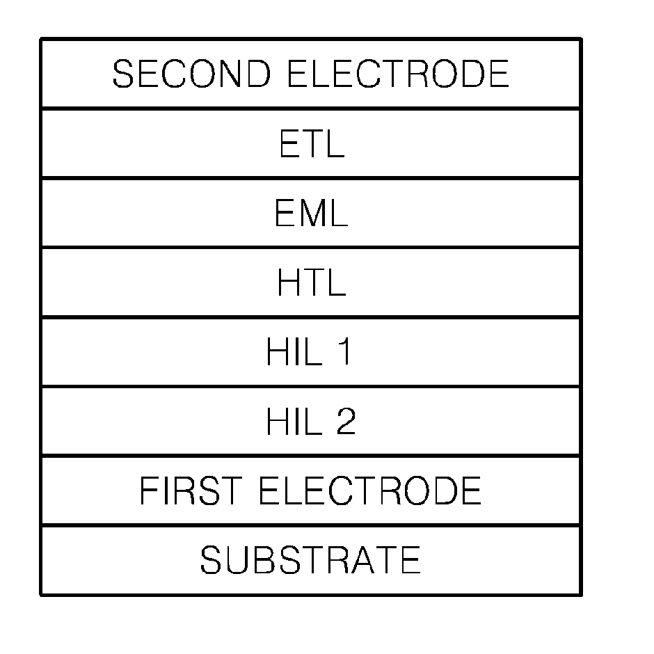
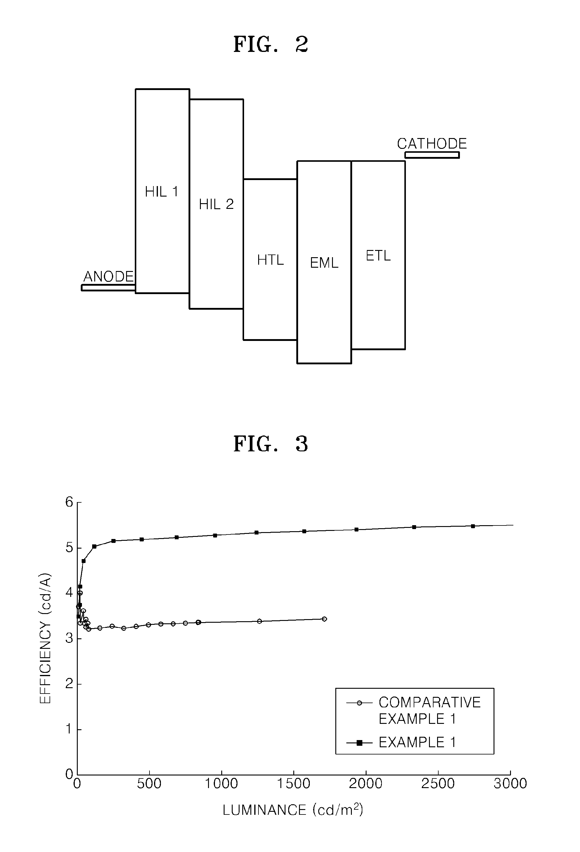
[0073]An anode was prepared by cutting a Corning 150 cm2 (1200 Å) ITO glass substrate into a size of 50 mm×50 mm×0.7 mm, sonicating the substrate for 5 minutes using isopropyl alcohol and deionized water, irradiating the substrate with UV light for 30 minutes, and exposing the substrate to ozone.

[0074]First, NPB and MgF2 were co-deposited on the substrate to form an HIL 1 with a thickness of 50 Å. Next, molybdenum oxide and m-MTDATA were co-deposited on the HIL 1 to form an HIL 2 with a thickness of 600 Å. NPB was vacuum-deposited on the HIL 2 to form an HTL with a thickness of 40 nm. After forming the HTL as described, 100 parts by weight of Alq3 as a host, and 3 parts by weight of C545T as a dopant were vacuum-deposited on the HTL to form an EML. Then, 50 parts by weight of CsF and 50 parts by weight of Alq3 were vacuum co-deposited on the EML to form an ETL with a thickness of 35 nm. Then, the organic light-emittin...

Example

EXAMPLE 2

Manufacturing Example of Organic Light-Emitting Device

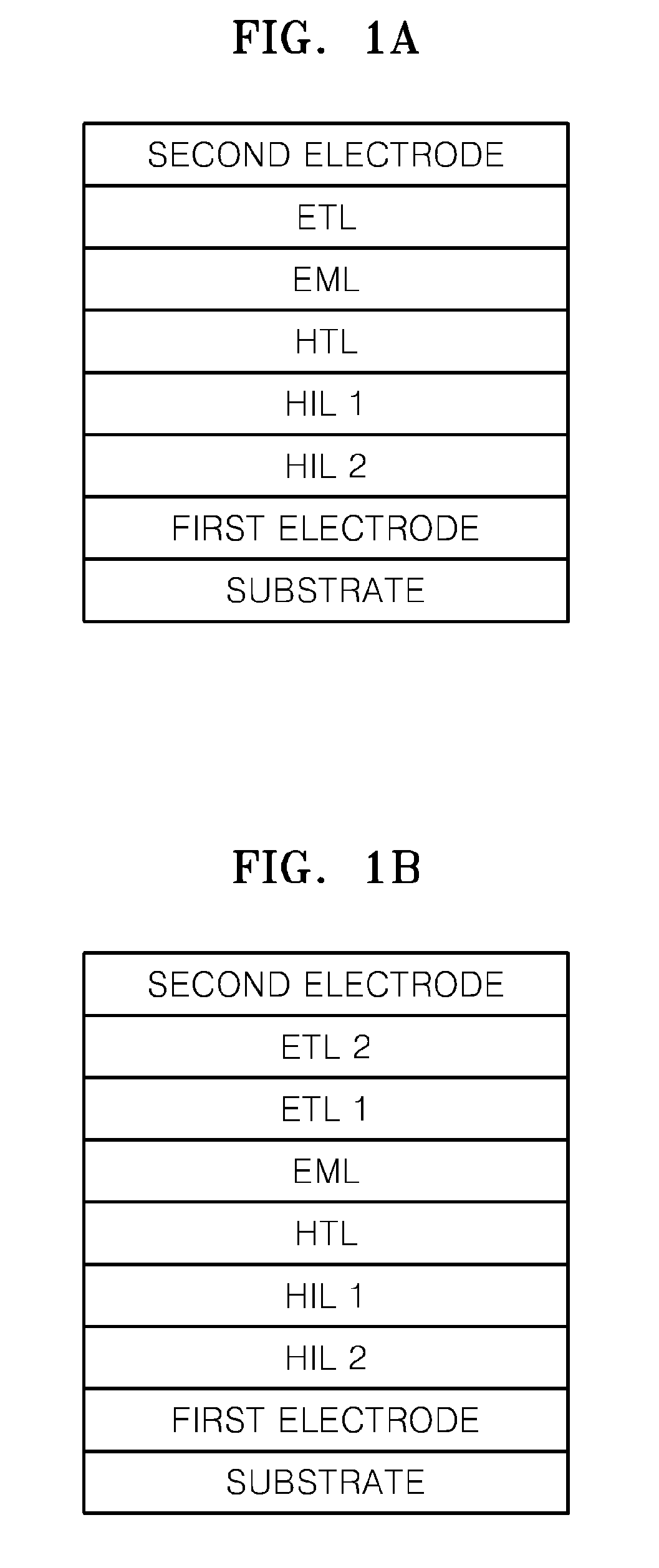
[0075]An organic light-emitting device was produced using the same method as in Example 1, except that the ETL of Example 2 was formed by vacuum co-depositing 50 parts by weight of lithium fluoride and 50 parts by weight of Alq3.

Example

COMPARATIVE EXAMPLE 1

Manufacturing Example of Organic Light-Emitting Device

[0076]An organic light-emitting device was produced using the same method as in Example 1, except that the ETL of the Comparative Example 1 only included Alq3.

[0077]The current efficiencies (cd / A) and power efficiencies (Im / W) with respect to the luminance (cd / m2) of the organic light-emitting devices produced according to Example 1 and Comparative Example 1 were investigated, and the results are shown in FIGS. 3 and 4, respectively. As shown in FIGS. 3 and 4, the Example 1, according to aspects of the present invention, exhibited a current efficiency and a power efficiency about 1.6 and 2 times greater, respectively, than the Comparative Example 1.

[0078]According to aspects of the present invention, an organic light-emitting device has excellent electrical characteristics, and uses a hole injecting material suitable for fluorescent and phosphorescent elements of all colors including red, green, blue, and whi...


PUM


Abstract

An organic light-emitting device comprising: a first electrode; a second electrode; an emissive layer; a first hole injecting layer disposed between the first electrode and the emissive layer; a second hole injecting layer disposed between the first electrode and the emissive layer; and an electron transporting layer disposed between the emissive layer and the second electrode, wherein the first hole injecting layer comprises a metal fluoride, the second hole injecting layer comprises molybdenum oxide, and the electron transporting layer comprises a metal compound represented by Formula 1 below:
XaYb   <Formula 1>
X is one of an alkaline metal, an alkaline earth metal, and a transition metal,
Y is one of a Group 7 element and a C1-C20 organic group,
    • a is 1 to 3, and
    • b is 1 to 3.

Description

CROSS-REFERENCE TO RELATED APPLICATION[0001]This application claims the benefit of Korean Patent Application No. 2008-19618, filed on Mar. 3, 2008 in the Korean Intellectual Property Office, the disclosure of which is incorporated herein by reference.BACKGROUND OF THE INVENTION[0002]1. Field of the Invention[0003]Aspects of the present invention relate to an organic light-emitting device, and more particularly, to an organic light-emitting device with improved driving voltage, light emitting efficiency, and life span characteristics. Aspects of the present invention relate to developing a premium organic light-emitting device, which includes a decrease in power consumption and life span improvement of the organic light-emitting device.[0004]2. Description of the Related Art[0005]Organic light-emitting devices emit light by a coupling of electrons and holes in an organic film disposed between two electrodes when a voltage potential is applied to the organic film Organic light-emittin...

Claims


Application Information

Patent Timeline
IPC IPC(8): H01J1/63
CPCH01L51/001H01L51/002H01L51/0081H01L2251/558H01L51/5088H01L2251/308H01L51/5048H10K71/164H10K71/30H10K85/324H10K50/14H10K50/17H10K2102/103H10K2102/351H05B33/20H10K50/00
Inventor SONG, WON-JUNPARK, SOO-JIN
Owner SAMSUNG MOBILE DISPLAY CO LTD
Why Eureka
Try Eureka