Different metallic thin plates welding method, bimetallic thin plates jointing element, electric device, and electric device assembly

a technology of bimetallic thin plates and welding methods, which is applied in the direction of cell components, cell component details, manufacturing tools, etc., can solve the problems of deterioration of electric characteristics at connecting parts, and achieve the effect of sufficient electric characteristics and sufficient electric characteristics

Inactive Publication Date: 2009-09-10
NEC CORP +1
View PDF5 Cites 43 Cited by
  • Summary
  • Abstract
  • Description
  • Claims
  • Application Information

AI Technical Summary

Benefits of technology

[0013]In the bimetallic thin plate jointing element according to the present invention, the metallic thin plates are jointed to each other by a plurality of the spot-like welding areas. Therefore, compared to a conventional constitution in which the metallic thin plates are jointed by a continuous welding area, the total mass of the welding areas themselves, i.e., a total mass of the alloyed materials, is reduced, so that any increase of electric resistance by the alloyed materials can be restrained. Also, an area between the welding areas in a closely-jointed surface of the metallic thin plates has a condition in which the metallic thin plates are directly and stably jointed closely to each other, so that any increase of electric resistance can be restrained. Furthermore, because the spot-like welding areas have a tapered cross sectional shape, the diameter of the welding area on the closely-jointed surface of the metallic thin plates is comparatively small, so that the area between the welding areas can be kept large.
[0014]In the welding method according to the present invention, the above-mentioned bimetallic thin plate jointing element according to the present invention can be reliably manufactured. Also, compared to a conventional structure for forming a continuous welding area, this welding method for forming a plurality of spot-like welding areas can reduce energy required for forming the welding areas. In particular, laser beams are irradiated from a low melting-point member side, so that the welding areas can be formed with less energy than that when irradiated from a high melting-point member side.
[0017]As described above, in the method for welding different metallic thin plates according to the present invention, a plurality of spot-like welding areas have a cross sectional shape which is tapered from one thin plate toward the other thin plate, so that the total mass of the welding areas made of the alloyed material is reduced, and an area where metallic thin plates come into direct and close contact to each other is secured between the welding areas, as a result of which the metallic thin plates can be jointed to each other while keeping a sufficient electric characteristic. Accordingly, the bimetallic thin plate jointing element according to the present invention which can be manufactured by such a welding method has a sufficiently maintained electric characteristics. If such a jointing element is used as a terminal of the electric device, an electric device assembly with a sufficiently kept electric characteristic at a connection part of the terminals can be provided.

Problems solved by technology

Normally, electric resistance is increased at an alloyed portion, which leads to possibility of deteriorating an electric characteristic at a connecting part.

Method used


Image

  • Different metallic thin plates welding method, bimetallic thin plates jointing element, electric device, and electric device assembly
  • Different metallic thin plates welding method, bimetallic thin plates jointing element, electric device, and electric device assembly
  • Different metallic thin plates welding method, bimetallic thin plates jointing element, electric device, and electric device assembly

Examples


Embodiment Construction

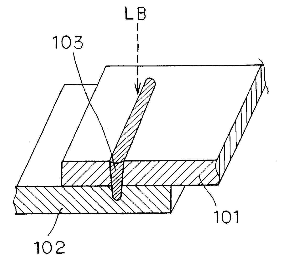
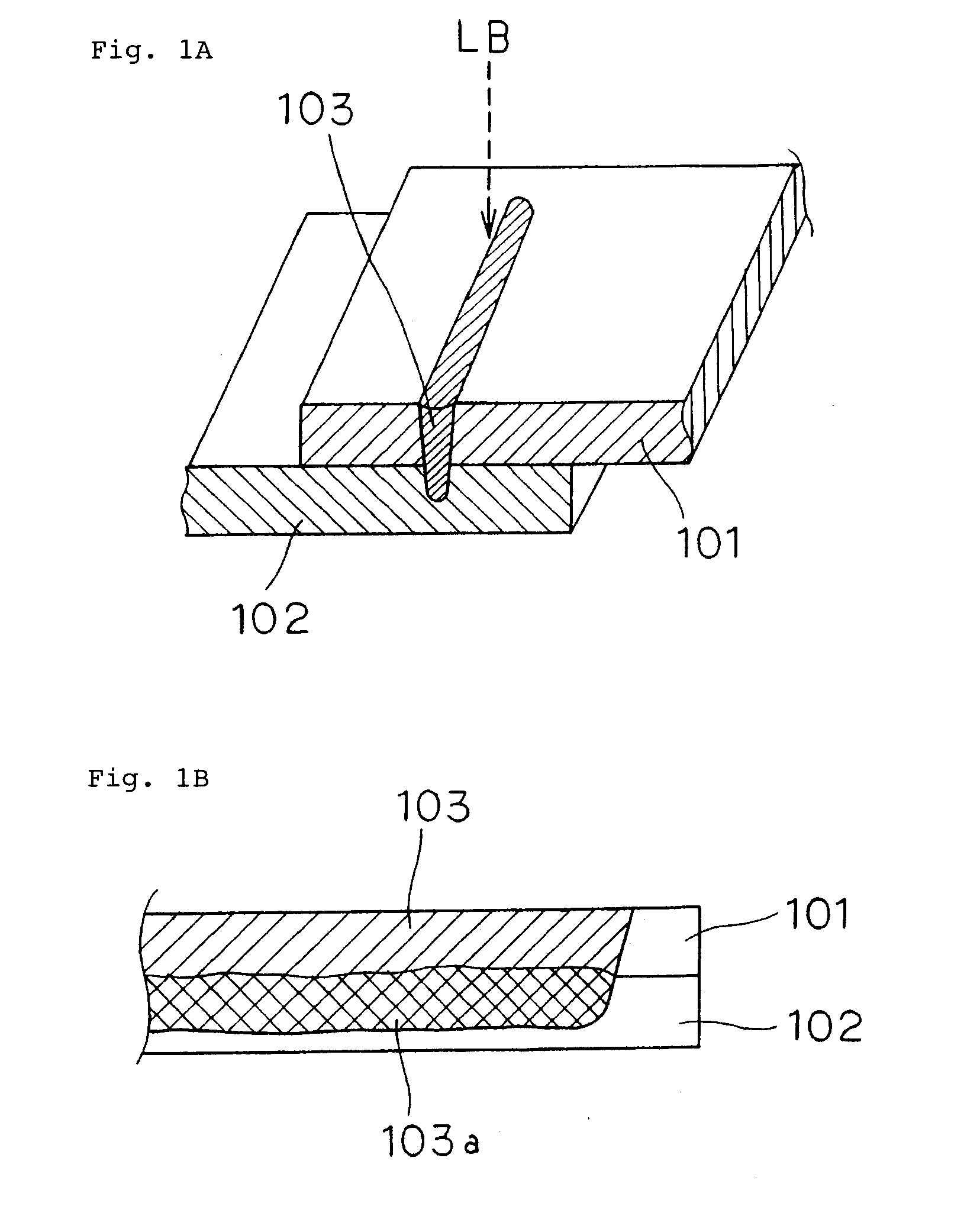
[0042]Now, an embodiment of the present invention will be explained with reference to the drawings. FIG. 3 is a perspective view showing one embodiment of an assembled battery according to the present invention.

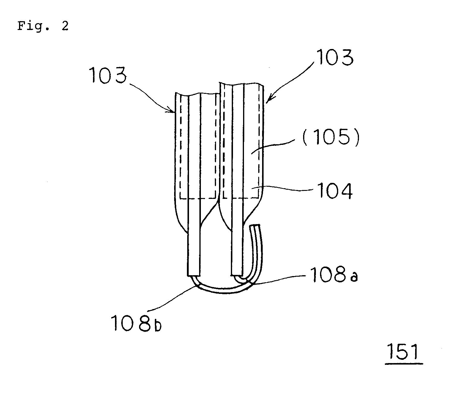
[0043]As shown in FIG. 3, assembled battery 50 is an electric device assembly which is configured by serially connecting a plurality of laminated battery cells 20 (electric devices). In FIG. 3, laminated battery cells 20 are shown as aligned in a line, but may be overlaid on each other when needed.

[0044]One laminated battery cell 20 has a generating unit (electric device element) not shown, which is hermetically sealed by outer capsule 4, and positive-electrode terminal 1 and negative-electrode terminal 2 that are electrically connected with the inside generating unit are extended from the periphery of the outer capsule 4. Also, in illustrated thin plate jointing element 10, positive-electrode terminal 1 and negative-electrode terminal 2 are jointed to each other by welding, ...


PUM

PropertyMeasurementUnit
aspect ratioaaaaaaaaaa
thicknessaaaaaaaaaa
thicknessaaaaaaaaaa

Abstract

A bimetallic thin plate jointing element that is jointed, such that a good electric characteristics are maintained, is provided. Thin plate jointing element (10) is formed by welding and jointing positive-electrode terminal (1) and negative-electrode terminal (2) having different melting points, and having flexibility. A plurality of spot-like welding areas (3) formed, for example, by laser welding are provided at overlaid portion (9) of positive-electrode terminal (1) and negative-electrode terminal (2). Welding areas (3) are formed by irradiating laser beams from the side of positive-electrode terminal (1) having a relatively low melting point, and have a cross sectional shape that is tapered from the side of positive-electrode terminal (1) side toward negative-electrode terminal (2).

Description

TECHNICAL FIELD[0001]The present invention relates to a welding method for irradiating laser beams or electron beams and jointing metallic thin plates of different materials using heat generated at that time, a bimetallic thin plate jointing element jointed by this method, an electric device which uses the bimetallic thin plate jointing element as a terminal, and an electric device assembly.BACKGROUND ART[0002]Conventionally, laser welding for jointing metallic plates by irradiating laser beams is known. FIG. 1 explains laser welding, FIG. 1A is a perspective view, and FIG. 1B is a cross section view showing a welding area along a longitudinal direction. Additionally, such laser welding is disclosed in Japanese Patent Laid-Open No. 300086 / 97.[0003]As shown in FIG. 1A, laser welding is done by partially overlaying two metallic plates 101 and 102 to each other, and irradiating laser beams to that overlaid portion from above. That is to say, upper metallic plate 101 is heated by the ir...

Claims


Application Information

Patent Timeline
Patent Type & Authority Applications(United States)
IPC IPC(8): B23K26/00B23K9/00H01M50/105H01M50/516
CPCB23K15/008B23K15/0093B23K26/22B23K26/40B23K2201/36B23K26/246H01M2/0207H01M2/202H01M2/206H01R4/625H01R43/0221B23K2203/18B23K26/244B23K2101/36B23K2103/10B23K2103/12B23K2103/18Y02E60/10H01M50/105H01M50/516
Inventor HOSOYA, TOSHIZO
Owner NEC CORP
Why Eureka
Try Eureka