Image sensor using back-illuminated photodiode and method of manufacturing the same

a photodiode and image sensor technology, applied in the field of image sensors, can solve the problems of color crosstalk, deterioration, heat treatment cannot be performed at a high temperature, and light sensitivity, so as to reduce noise and crosstalk and improve sensitivity.

Active Publication Date: 2009-09-10
SK HYNIX INC
View PDF6 Cites 74 Cited by
  • Summary
  • Abstract
  • Description
  • Claims
  • Application Information

AI Technical Summary

Benefits of technology

[0011]The present invention provides an image sensor using a back-illuminated photodiode which absorbs light through its bottom side instead of its top side, restricts the generation of noise and crosstalk by treating a wafer surface, and thus improves sensitivity, and a method of manufacturing the image sensor.

Problems solved by technology

Throughout this process, sensitivity of light, particularly, blue light, deteriorates.
This affects an adjacent photodiode, resulting in a color crosstalk.
However, there has been a problem in that heat treatment cannot be performed at a high-temperature because of the existing metal wire.
Therefore, the conventional image sensor using the back-illuminated photodiode cannot solve a noise problem that is resulted from a defected surface of a silicon substrate on which the back-illuminated photodiode is formed.
To address this problem, laser scanning is generally used for instantaneous high-temperature heat treatment, which is disadvantageously expensive and time consuming.

Method used


Image

  • Image sensor using back-illuminated photodiode and method of manufacturing the same
  • Image sensor using back-illuminated photodiode and method of manufacturing the same
  • Image sensor using back-illuminated photodiode and method of manufacturing the same

Examples


Embodiment Construction

[0022]Hereinafter, exemplary embodiments of the present invention will be described in detail with reference to the accompanying drawings.

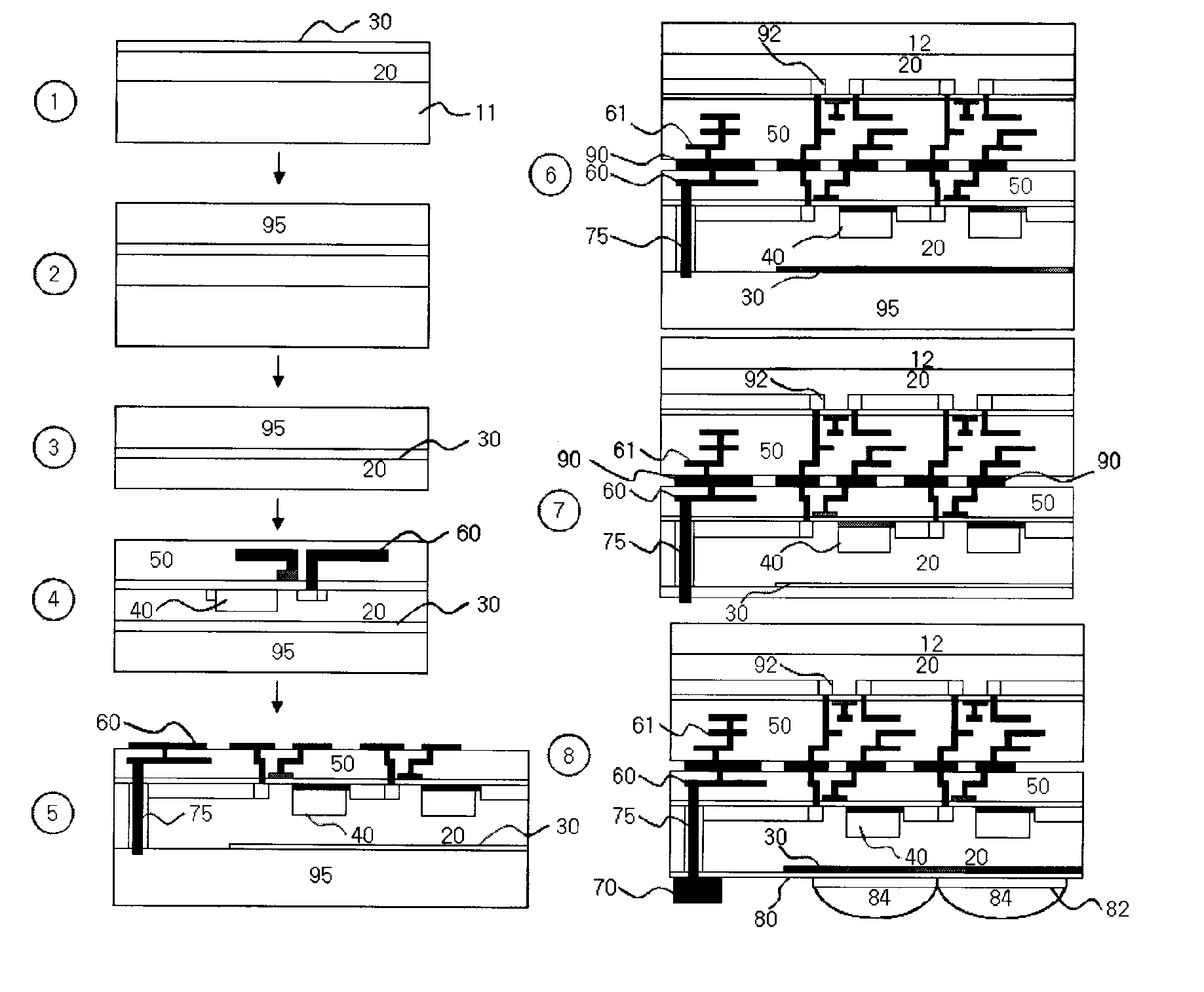
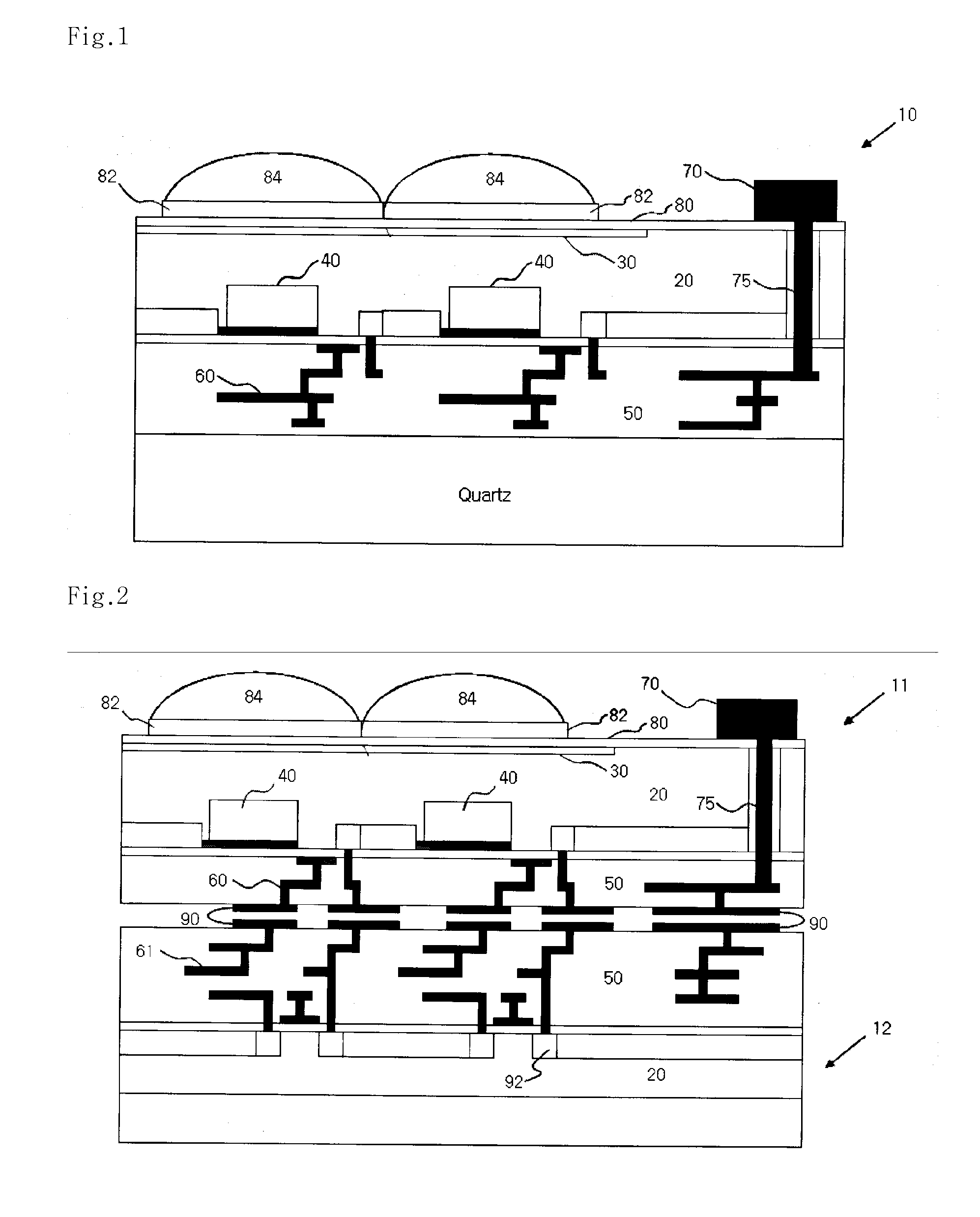
[0023]FIG. 1 is a cross-sectional view of a structure of an image sensor using a back-illuminated photodiode according to an embodiment of the present invention. The image sensor is formed of a specific type of wafer 10, an epitaxial layer (or epi-layer) 20, a potential barrier 30, a back-illuminated photodiode 40, an inter-metal dielectric (IMD) layer 50, a metal wire 60, a pad 70, a via & plug 75, a passivation layer 80, a color filter 82, and a micro-lens 84.

[0024]The potential barrier 30 is formed on a surface of the epi-layer 20 with low concentration by doping impurities having the same type as the epi-layer 20 and having higher concentration than the epi-layer 20.

[0025]The potential barrier 30 may be formed by using ion implantation, epitaxial growth, or boro silicate glass (BSG) deposition.

[0026]The back-illuminated photodiode 40 is formed...


PUM


Abstract

An image sensor using a back-illuminated photodiode and a manufacturing method thereof are provided. According to the present invention, since a surface of the back-illuminated photodiode can be stably treated, the back-illuminated photodiode can be formed to have a low dark current, a constant sensitivity of blue light for all photodiodes, and high sensitivity. In addition, it is possible to manufacture an image sensor with high density by employing a three dimensional structure in which a photodiode and a logic circuit are separately formed on different substrates.

Description

BACKGROUND OF THE INVENTION[0001]1. Field of the Invention[0002]The present invention relates to an image sensor, and more particularly, to an image sensor using a back-illuminated photodiode which absorbs light through its bottom side and a method of manufacturing the image sensor.[0003]2. Description of the Related Art[0004]A complementary metal-oxide semiconductor (CMOS) image sensor is a device for measuring light intensity. In general, such image sensor has a structure in which a photodiode is formed on a plane where a digital / analog circuit is formed, and a metal wire and an inter-metal dielectric (IMD) layer are formed on a top side of the photodiode.[0005]In the conventional image sensor, light passes through a micro-lens and a color filter and thereafter proceeds along a pathway of several films before being absorbed by the photodiode. Throughout this process, sensitivity of light, particularly, blue light, deteriorates.[0006]Furthermore, in the conventional image sensor, a...

Claims


Application Information

Patent Timeline
Patent Type & Authority Applications(United States)
IPC IPC(8): H01L31/0232H01L31/102
CPCH01L27/14621H01L27/14627H01L27/14687H01L27/14636H01L27/1464H01L27/14632H01L27/146
Inventor LEE, BYOUNG SUWON, JUN HO
Owner SK HYNIX INC
Why Eureka
Try Eureka