Semiconductor Wafer Of Single Crystalline Silicon and Process For Its Manufacture

Active Publication Date: 2009-09-10
SILTRONIC AG
View PDF3 Cites 5 Cited by
  • Summary
  • Abstract
  • Description
  • Claims
  • Application Information

AI Technical Summary

Benefits of technology

[0008]It is an object of the present invention to avoid defects rated as disturbing of agglomerated intrinsic point defects in semiconductor wafers composed of silicon in a reliable and simple manner, and to open up particularly economic a

Problems solved by technology

These defects are normally not acceptable at all.
If a dominant type of point defect attains supersaturation during cooling, agglomerates of this type of point defect can arise.
However, single crystals having diameters of 200 mm or greater cannot be cooled arbitrarily rapidly, with the result that limits are imposed on controlling the size of defects by limiting

Method used


Image

  • Semiconductor Wafer Of Single Crystalline Silicon and Process For Its Manufacture
  • Semiconductor Wafer Of Single Crystalline Silicon and Process For Its Manufacture

Examples


example 1

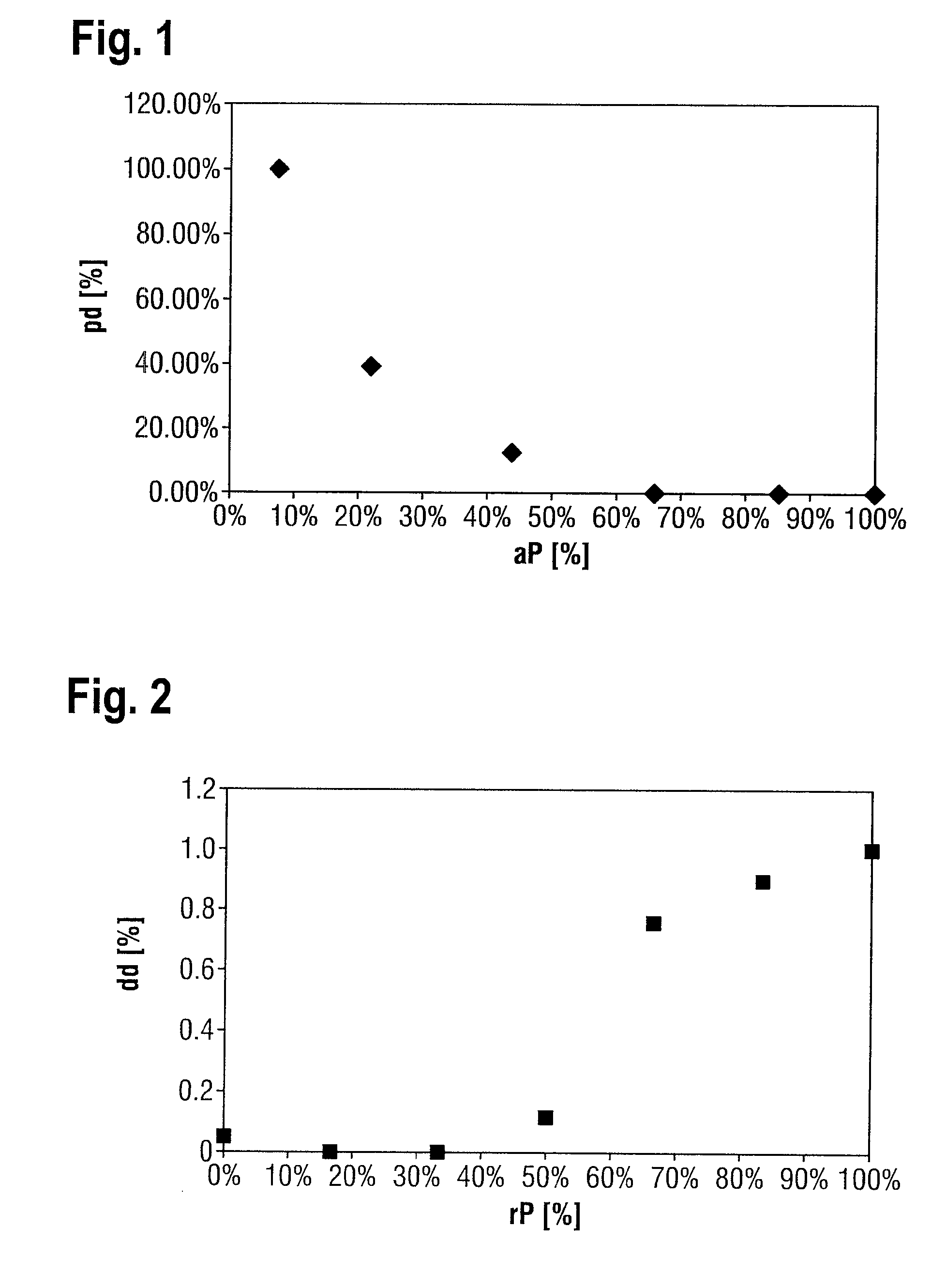
[0030]A single-crystal rod composed of silicon was pulled in accordance with the FZ method, to be precise, firstly in an atmosphere comprising argon. The melt was doped neither with nitrogen nor with hydrogen. After a pulled rod length of 10 cm having a nominal diameter, SiF4 as fluorine source was conducted into the atmosphere and the concentration was increased continuously from 0.6 l / h to 5 l / h up to a pulled rod length of 50 cm. Another 10 cm of rod length were then pulled without supply of SiF4 and with a stationary gas atmosphere. The entire single crystal remained free of dislocations. The subsequent analysis with regard to Lpit defects after Secco etch by visual inspection and with regard to COP defects by infrared laser scattered light tomography using an analysis device of the MO-4 type from the manufacturer Mitsui Mining and Smelting, Japan, revealed that the Lpit defects initially present in the edge region of the single crystal disappeared first and the COP defects pres...

example 2

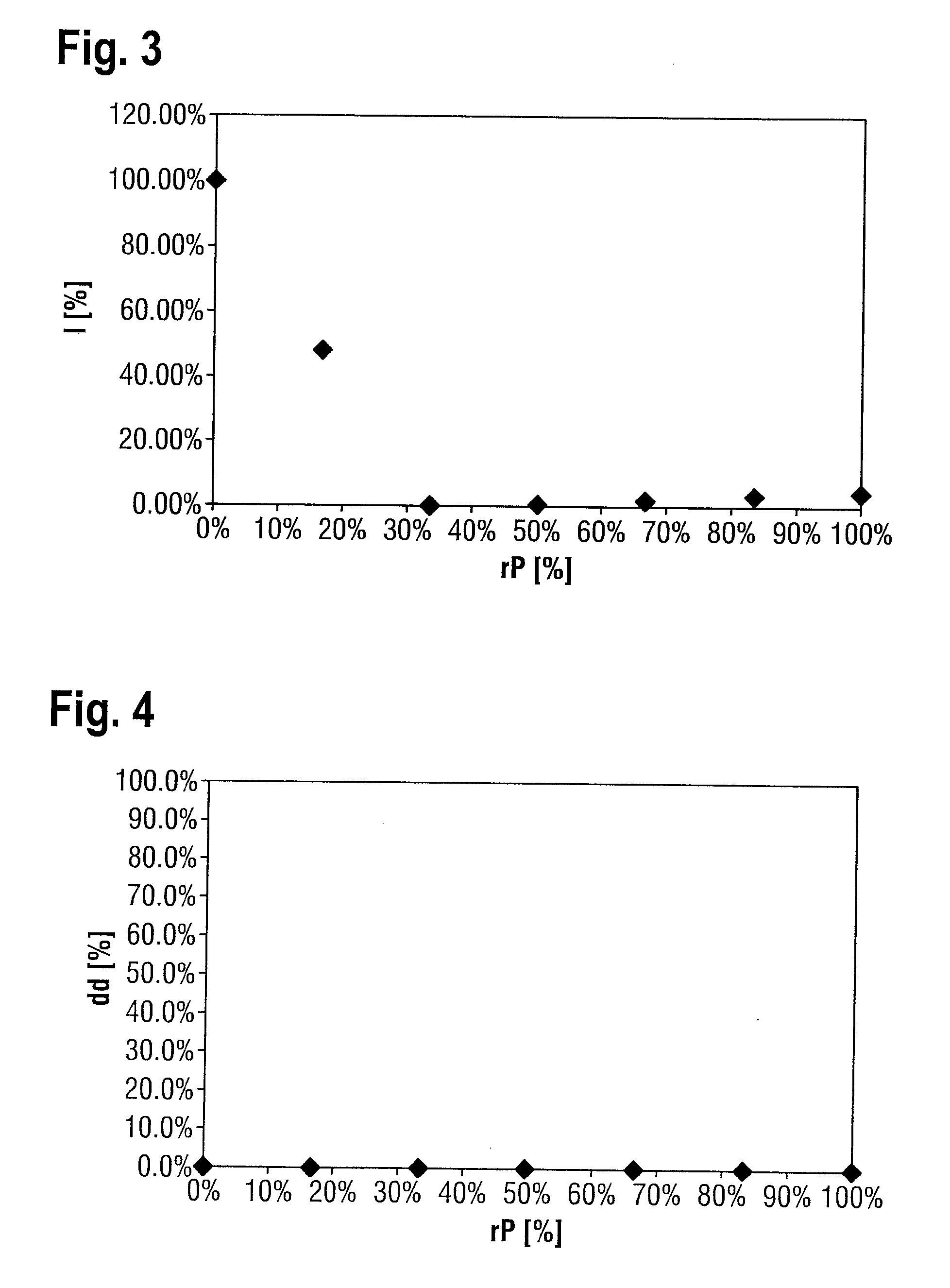
[0033]A single crystal composed of silicon having a length of 1 m and a diameter of 300 mm was pulled in accordance with the CZ method. Initially only argon was conducted through the pulling device. The melt was doped neither with nitrogen nor with hydrogen. After a pulled rod length of 20 cm having a nominal diameter was reached, SiF4 as fluorine source was conducted in addition to argon through the pulling device and the SiF4 flow rate was increased continuously from 30 l / h to 300 l / h. In this experiment, too, the increase in the fluorine concentration in the single crystal brought about the suppression of Lpit defects and COP defects initially present.


PUM


Abstract

Semiconductor wafer of monocrystalline silicon contain fluorine, the fluorine concentration being 1·1010 to 1·1016 atoms/cm3, and is free of agglomerated intrinsic point defects whose diameter is greater than or equal to a critical diameter. The semiconductor wafers are produced by providing a melt of silicon which is doped with fluorine, and crystallizing the melt to form a single crystal which contains fluorine within the range of 1·1010 to 1·1016 atoms/cm3, at a growth rate at which agglomerated intrinsic point defects having a critical diameter or larger would arise if fluorine were not present or present in too small an amount, and separating semiconductor wafers from the single crystal.

Description

CROSS-REFERENCE TO RELATED APPLICATIONS[0001]This application claims the benefit of U.S. provisional application Ser. No. 61 / 035,056, filed Mar. 10, 2008, and claims priority to German application 10 2008 013325.6 filed Mar. 10, 2008, both of which are herein incorporated by reference.BACKGROUND OF THE INVENTION[0002]1. Field of the Invention[0003]The invention relates to a semiconductor wafer composed of silicon, which contains fluorine and is particularly suitable for producing electronic components because it has no agglomerated intrinsic point defects rated as disturbing. The invention also relates to a method for producing such a semiconductor wafer.[0004]2. Background Art[0005]Since the beginnings of microelectronics the manufacturers of semiconductor wafers composed of silicon have devoted themselves particularly to the task of eliminating defects rated as disturbing, at least in that region of the semiconductor wafer in which the construction of structures of electronic comp...

Claims


Application Information

Patent Timeline
IPC IPC(8): H01L29/167H01L21/38
CPCC30B29/06C30B15/04C01B33/00C07F7/12H01L21/18H01L21/208
Inventor VON AMMON, WILFRIED
Owner SILTRONIC AG
Why Eureka
Try Eureka