Thin film transistor array substrate and manufacturing method thereof

a technology of thin film transistors and array substrates, which is applied in the direction of optics, semiconductor devices, instruments, etc., can solve the problems of difficult to ensure yield and product quality, decrement of electrical characteristics uniformity of tft across the whole substrate, and difficulty in ensuring yield and product quality. , to achieve the effect of improving the product yield and quality of tft array substrates, improving the uniformity of electrical characteristics of tft, and improving the channel length o

Active Publication Date: 2009-09-10
BEIJING BOE OPTOELECTRONCIS TECH CO LTD +1
View PDF1 Cites 25 Cited by
  • Summary
  • Abstract
  • Description
  • Claims
  • Application Information

AI Technical Summary

Benefits of technology

[0011]The embodiments of the invention provide a TFT array substrate for a LCD and a manufacturing method thereof. A four-mask process is adopted; however it is different from the conventional four-mask process using a gray tone mask. Specifically, in the embodiments of the invention, the structure of the data line PAD region is formed with a gray tone process, and the TFT channel is formed through the conventional photolithography and etching process, so that the defects of the pixels in the conventional four-mask process using a gray tone mask can be efficiently reduced, which improves the product yield and quality of the TFT array substrate for a LCD. At the same time, since the TFT channel is formed through the conventional photolithography, the uniformity of the channel length of the TFT can be improved, and the uniformity of the electrical characteristics of the TFT can be improved. The manufacturing method of the TFT array substrate structure for a LCD according to the embodiment is simple, stable and easy to realize, which decreases the requirement on equipment, reduces product period and decreases product cost.

Problems solved by technology

Due to a limitation on the accuracy of manufacturing a mask with slits and the influence of the distribution uniformity of the transmission of the mask and the uniformity of the subsequent photoresist ashing process, there exists some difference for the transmission in different areas, and this difference may in turn cause the various defects in the TFT channel, decreasing the electrical characteristics uniformity of the TFT across the whole substrate and degrading the display quality of the TFT-LCD.
These etching processes are performed in the same apparatus sequentially, which tends to cause the various kinds of defects in pixels because of the slit photolithography process, so that the yield and the product quality are difficult to be ensured.

Method used


Image

  • Thin film transistor array substrate and manufacturing method thereof
  • Thin film transistor array substrate and manufacturing method thereof
  • Thin film transistor array substrate and manufacturing method thereof

Examples


first embodiment

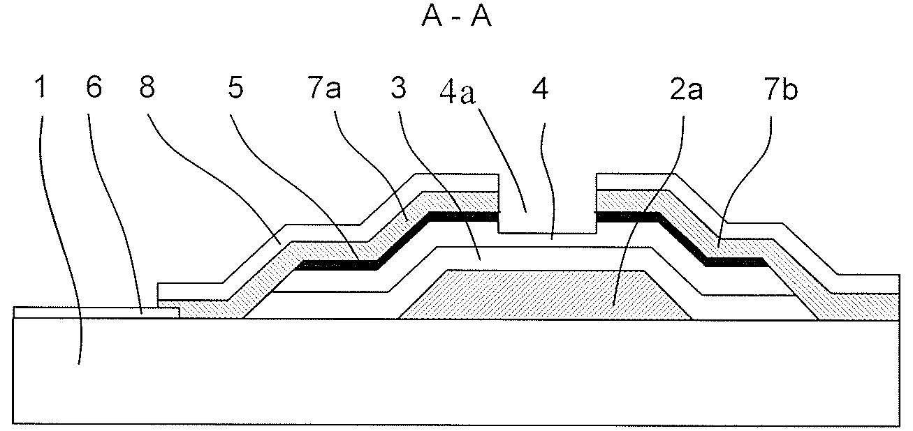
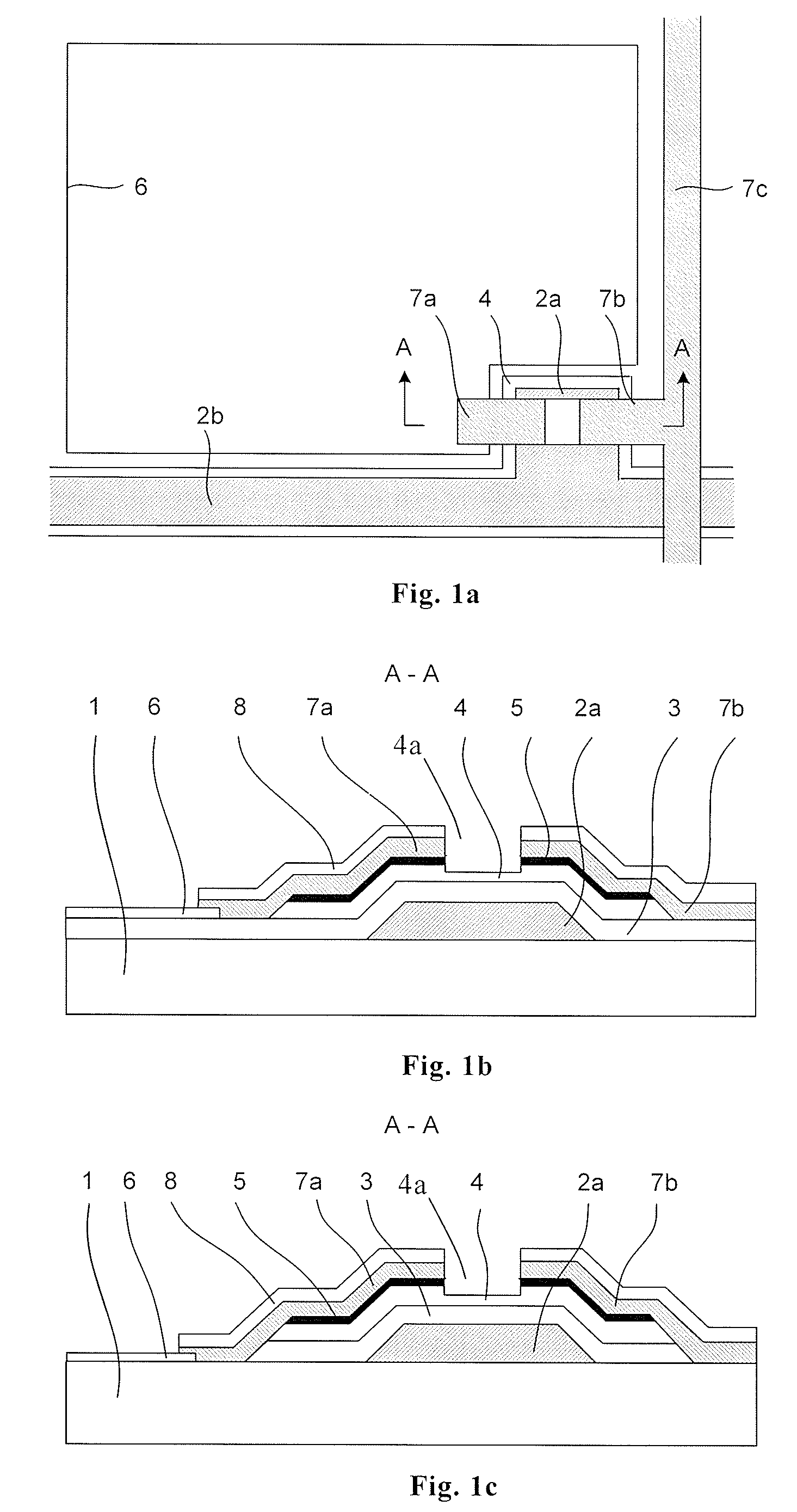
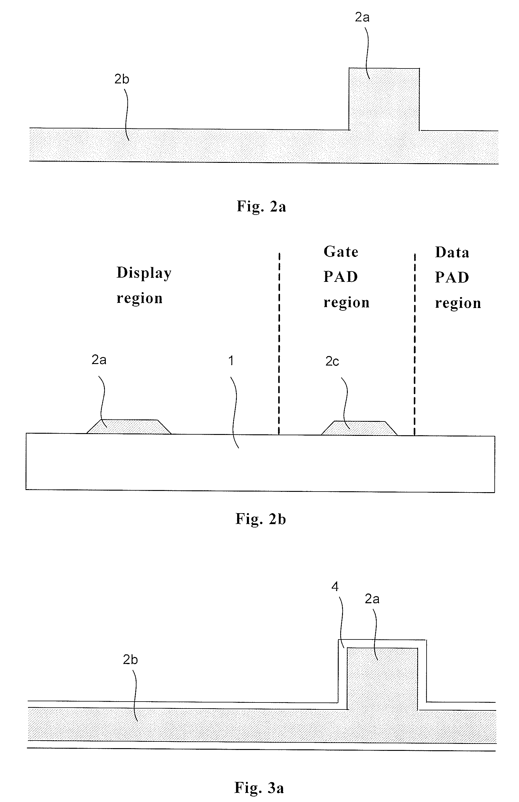
[0042]FIG. 2a is a plan view of the first embodiment after a first patterning process in the embodiment, and FIG. 2b is a cross-sectional view of a display region, a gate line PAD region and a data line PAD region in the structure in FIG. 2a. A gate metal layer is deposited on the base substrate 1 (e.g., a glass substrate, a quartz substrate, or a plastic substrate) to a thickness of 500 Ř4000 Šby a sputtering method or a thermal evaporation method. The gate metal layer may be a metal such as Cr, W, Ti, Ta, Mo, Al, Cu or an alloy thereof, and the gate metal layer may also be a multi-layer metal thin film. The gate metal layer is etched through the first patterning process to form a pattern of a gate electrode 2a and a gate line 2b on the display region and form a pattern of a gate connecting line 2c in the gate line PAD region on the base substrate 1, as shown in FIGS. 2a and 2b.

[0043]FIG. 3a is a plan view of the first embodiment after a second patterning process, and FIG. 3b is...


PUM

PropertyMeasurementUnit
lengthaaaaaaaaaa
lengthaaaaaaaaaa
transparentaaaaaaaaaa

Abstract

A thin film transistor (TFT) array substrate for a liquid crystal display comprises a gate line and a data line formed in a display region, a gate connecting line and a data connecting line formed in a PAD region, and a TFT formed at an intersection between the gate line and the data line. The TFT comprises a gate electrode on a base substrate, a gate insulating layer on the gate electrode, a semiconductor layer on the gate insulating layer, a doped semiconductor layer on the semiconductor layer, and a source electrode and a drain electrode that are on the doped semiconductor layer, and a TFT channel is defined in the semiconductor layer between the source electrode and the drain electrode. The array substrate further comprises a passivation layer that is formed on the source electrode and the drain electrode and a pixel electrode, a portion of which is formed under the drain electrode and connected with the drain electrode.

Description

FIELD OF THE INVENTION[0001]The present invention relates to a thin film transistor liquid crystal display (TFT-LCD) and a manufacturing method thereof.BACKGROUND OF THE INVENTION[0002]A thin film transistor liquid crystal display (TFT-LCD) has many merits such as small volume, lower power consumption, and being free of radiation and is gaining a important role in the flat panel display market. As for a TFT-LCD, product quality, yield and price are mainly determined by the structure and the manufacturing process of an array substrate structure thereof.[0003]In order to effectively decrease price and increase yield of a TFT-LCD, the process of manufacturing the array substrate (active matrix driven TFT array) of a TFT-LCD has been simplified gradually. The method has been developed from the initial seven-mask process to the current four-mask process that is based on slit photolithography technology. The key points of the four-mask process is to use a slit photolithography process to ...

Claims


Application Information

Patent Timeline
Patent Type & Authority Applications(United States)
IPC IPC(8): G02F1/136H01L21/336
CPCG02F1/1368H01L27/1288H01L27/124G02F2001/136236G02F1/136236
Inventor WANG, ZHANGTAOQIU, HAIJUNMIN, TAE YUP
Owner BEIJING BOE OPTOELECTRONCIS TECH CO LTD
Why Eureka
Try Eureka