Photomask blank, photomask, and photomask manufacturing method

a technology of photomask and manufacturing method, which is applied in the field of photomask blank, photomask, and photomask manufacturing method, can solve the problems of difficult to prevent the collapse of resist pattern, the inability to form satisfactorily desired fine patterns, etc., and achieve the effect of reducing the light-shielding performance or the etching performance of ta metal, improving the smoothness of light-shielding film, and reducing the light-shielding performance of

Active Publication Date: 2009-09-10
HOYA CORP
View PDF4 Cites 18 Cited by
  • Summary
  • Abstract
  • Description
  • Claims
  • Application Information

AI Technical Summary

Benefits of technology

[0016]Therefore, if the same material as that of the front-surface antireflection layer is used as means for controlling the back-surface reflectance, another etching process is further added. This increases uncertainty of the processes, complicates the structure of an apparatus to be used, and increases not a little the manufacturing cost. Further, since a synthetic quartz glass generally used as a transparent substrate of an ultraviolet light mask can be etched with the fluorine-based gas, if the back-surface antireflection layer formed on the transparent substrate is etched with the fluorine-based gas, there occurs a phenomenon that the glass is damaged, which causes an adverse influence on exposure.
[0017]In view of this, as a result of studying a material that does not need such an etching gas for etching thereof and is still capable of obtaining the back-surface antireflection effect, it has been found that Ta nitride is optimal. It has been found that although Ta nitride does not have sufficient optical properties for ArF exposure light as the front-surface antireflection layer, it exhibits a sufficient antireflection effect as the back-surface antireflection layer formed on the transparent substrate made of synthetic quartz or the like and, by adjusting the N content of the Ta nitride layer, it is fully possible to set the back-surface reflectance to less than 40%. Further, it has been found that, by adjusting the composition of Ta nitride, sufficient light-shielding performance can be obtained as the light-shielding layer and, simultaneously, sufficient antireflection performance can be obtained as the back-surface antireflection layer, and therefore, since the functions of the light-shielding layer and the back-surface antireflection layer can be achieved by the single layer, it is possible to realize a light-shielding film with a two-layer structure in which the back-surface antireflection layer is omitted.
[0037]In the above aspects, the light-shielding layer mainly contains Ta nitride (tantalum nitride) and contains less than 62 at % N (nitrogen). This makes it possible to suppress the back-surface reflectance of the light-shielding film to less than 40%. Preferably, the light-shielding layer contains 7 at % or more N.
[0042]B (boron), C (carbon), Si (silicon), or the like may be added to the layer mainly containing Ta nitride for improving the smoothness of the light-shielding film. Since these elements each reduce the light-shielding performance or the etching performance of the Ta metal, the addition amount thereof is preferably set to 20 at % or less. Specifically, if B or C is added, the light-shielding performance of the layer mainly containing Ta nitride decreases, while, if C or Si is added, the etching rate thereof decreases. B may also be added to the Ta oxide antireflection layer for improving the smoothness of the light-shielding film. B has only a small influence on the antireflection performance and the etching characteristics being the subject of this invention. It is said that the smoothness of the light-shielding film affects the edge roughness in pattern formation. Besides, if the surface roughness of the light-shielding film is large, surface-roughness shapes are detected as defects and, therefore, there arises a problem that the detection sensitivity for foreign matter cannot be enhanced, so that the quality control of photomask blanks becomes difficult. In the experiments leading to this invention, M1350 (trade name) manufactured by Lasertec Corporation was used as a defect inspection apparatus, wherein, with respect to a light-shielding film with a surface roughness Rms of as large as 0.84 nm, surface-roughness shapes were erroneously detected as defects even at a portion where there were no foreign matter. Therefore, in the case of using this defect inspection apparatus, the Rms value of the surface of the light-shielding film needs to be less than 0.84 nm so as to prevent the reduction in inspection sensitivity due to the surface roughness. Also in the case of using another defect inspection apparatus, it is necessary to adjust the surface roughness of the light-shielding film by adjusting the N content or adding B, C, Si, or the like so as to achieve the Rms value small enough to prevent the defect inspection apparatus from erroneously judging surface-roughness shapes to be defects. As a gas added in sputtering the layer mainly containing Ta oxide, use may be made of a gas containing oxygen such as CO2, NO2, or NO instead of O2. In this event, there is a case where C or N is contained in the film, but C or N has only a small influence on the antireflection performance and the etching rate of the Ta oxide layer.
[0043]Further, by forming the light-shielding film into a stacked structure comprising the light-shielding layer made of a material having a refractive index n of more than 1.65 and less than 2.44 and an extinction coefficient k of more than 1.70 and less than 2.50 and the front-surface antireflection layer made of a material having a refractive index n of 2.23 or more and 2.42 or less and an extinction coefficient k of 0.63 or more and 1.09 or less, even if the thickness of the entire light-shielding film is less than 65 nm, it is possible to satisfy all the conditions of a transmittance of 0.2% or less, a front-surface reflectance of less than 30%, and a back-surface reflectance of less than 40% with respect to ArF excimer laser exposure light. It is more preferable that a material having a refractive index n of 1.80 or more and 2.35 or less and an extinction coefficient k of 1.85 or more and 2.37 or less be selected as the light-shielding layer.

Problems solved by technology

However, it has been found, for example, that when fabricating a photomask adapted for exposing a fine pattern with a line width of 70 nm or less by the use of ArF exposure light, a desired fine pattern cannot be formed satisfactorily only with the use of a photomask blank having a known light-shielding film formed by using a material mainly containing Ta as described above.
(a) When the width of a resist pattern becomes ⅓ or less of the thickness of a resist film, a problem such as collapse or stripping of the resist pattern occurs and, therefore, it is necessary to set the relationship between the width of the resist pattern and the thickness of the resist film so as to prevent the occurrence thereof.
(b) The resist should remain until etching of a light-shielding film is finished and further until additional etching for adjusting the shape of a pattern is finished and, practically, nonuniformity of the etching rate due to the difference in pattern width is also taken into account, and therefore, the remaining thickness of the resist is preferably about half the thickness of the resist film before the etching. In the case of using a conventional light-shielding film mainly containing Cr, since the etching rate thereof is only 0.5 to 0.6 times that of the resist under the general etching conditions, it is necessary that the thickness of the resist film be set to no less than about 200 nm. Thus, when the minimum width of the pattern becomes less than about 70 nm, it is difficult to prevent collapse of the resist pattern.

Method used


Image

  • Photomask blank, photomask, and photomask manufacturing method
  • Photomask blank, photomask, and photomask manufacturing method
  • Photomask blank, photomask, and photomask manufacturing method

Examples


example 1

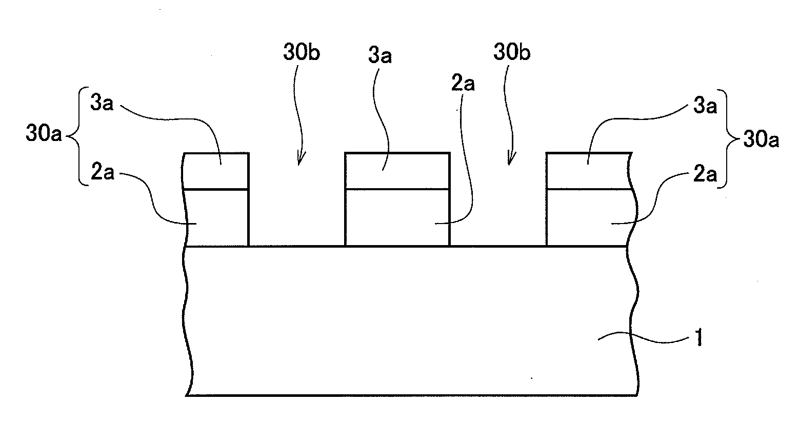
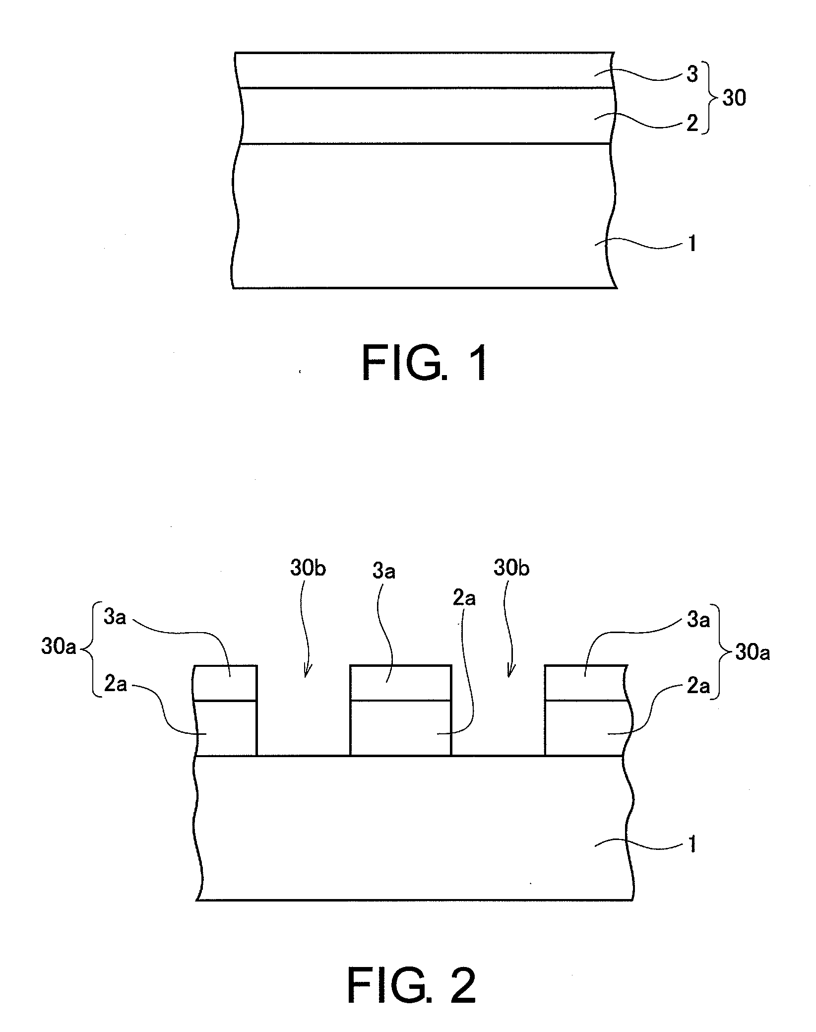
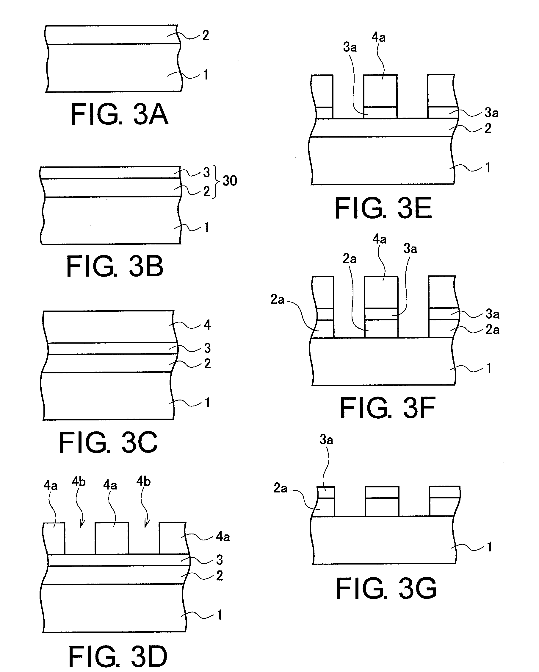
[0058]A substrate 1 made of synthetic quartz and having an about 152 mm×152 mm square size with a thickness of 6.35 mm was introduced into a DC magnetron sputtering apparatus. After the inside of the sputtering apparatus was evacuated to 2×10⁻⁵ (Pa) or less, a mixed gas (sputtering gas) of Ar and N2 was introduced into the sputtering apparatus. In this event, the flow rate of Ar and the flow rate of N2 were adjusted to 38.5 sccm and 9 sccm, respectively. Ta was used as a sputtering target. After the gas flow rates were stabilized, the power of a DC power supply was set to 1.5 kW, thereby forming a Ta nitride layer 2 having a thickness of 42.4 nm on the substrate 1 (see FIG. 3A).

[0059]Then, while the substrate 1 formed with the Ta nitride layer 2 was maintained in the sputtering apparatus, a mixed gas (sputtering gas) containing an Ar gas at a flow rate of 58 sccm and an O2 gas at a flow rate of 32.5 sccm was introduced into the sputtering apparatus and then the power of the DC power...

example 2

[0065]A photomask blank and a photomask according to Example 2 differ from Example 1 only in specific manufacturing conditions, but are the same in manufacturing sequence and so on. Therefore, specific manufacturing conditions and so on are shown in Table 3 to enable comparison with Example 1 and detailed explanation is omitted.

TABLE 3Introduced Gasduring SputteringConfiguration ofThicknessArN2O2Example 2Material(nm)(sccm)(sccm)(sccm)Front-SurfaceTa—O1358032.5AntireflectionLayerLight-ShieldingTa—N44.230200Layer

[0066]Further, the optical properties and so on of the photomask blank according to Example 2 are collectively shown in Table 4. Defect inspection was conducted using M1350 (trade name) manufactured by Lasertec Corporation and it was confirmed that it was possible to identify defects normally.

TABLE 4Optical PropertiesCompositionSurfaceFront-Back-NORoughnessProperties ofSurfaceSurfaceContentContentRmsExample 2ReflectanceReflectancenkTransmittance(at %)(at %)(nm)Front-Surface19....

example 3

[0067]A photomask blank and a photomask according to Example 3 differ from Examples 1 and 2 only in specific manufacturing conditions, but are the same in manufacturing sequence and so on. Therefore, specific manufacturing conditions and so on are shown in Table 5 to enable comparison with Examples 1 and 2 and detailed explanation is omitted.

TABLE 5Introduced Gasduring SputteringConfiguration ofThicknessArN2O2Example 3Material(nm)(sccm)(sccm)(sccm)Front-SurfaceTa—O1758032.5AntireflectionLayerLight-ShieldingTa—N46.220350Layer

[0068]Further, the optical properties and so on of the photomask blank according to Example 3 are collectively shown in Table 6. Defect inspection was conducted using M1350 (trade name) manufactured by Lasertec Corporation and it was confirmed that it was possible to identify defects normally.

TABLE 6Optical PropertiesCompositionSurfaceFront-Back-NORoughnessProperties ofSurfaceSurfaceContentContentRmsExample 3ReflectanceReflectancenkTransmittance(at %)(at %)(nm)Fr...


PUM

PropertyMeasurementUnit
thicknessaaaaaaaaaa
thicknessaaaaaaaaaa
thicknessaaaaaaaaaa

Abstract

A photomask blank has a light-shielding film composed of at least two layers on a transparent substrate. The light-shielding film includes a light-shielding layer made of a material mainly containing tantalum nitride and containing less than 62 at % nitrogen. The material is capable of being dry-etched with a chlorine-based gas containing no oxygen. The light-shielding film further includes a front-surface antireflection layer formed on the light-shielding layer and made of a material not capable of being dry-etched with a chlorine-based gas, but capable of being dry-etched with a fluorine-based gas.

Description

[0001]This application is based on and claims the benefit of priority from Japanese Patent Application No. 2008-046889, filed on Feb. 27, 2008, and Japanese Patent Application No. 2009-015733, filed on Jan. 27, 2009, the disclosures of which are incorporated herein in their entirety by reference.TECHNICAL FIELD[0002]This invention relates to a photomask for use as a mask in, for example, transferring a fine pattern in the manufacture of semiconductor devices and to a photomask blank as an intermediate product that can be formed into a photomask by applying certain treatments thereto, and further relates to a method of manufacturing a photomask.BACKGROUND ART[0003]Generally, in the manufacture of semiconductor devices or the like, a fine pattern is formed by photolithography and, in a fine pattern transfer process where the photolithography is performed, a photomask is used as a mask. The photomask is generally obtained by forming a desired fine pattern in a light-shielding film or t...

Claims


Application Information

Patent Timeline
Patent Type & Authority Applications(United States)
IPC IPC(8): G03F1/00G03F1/50G03F1/54H01L21/027
CPCG03F1/14G03F1/80G03F1/58G03F1/46G03F1/50H01L21/0276G03F1/62
Inventor NOZAWA, OSAMU
Owner HOYA CORP
Why Eureka
Try Eureka