

Semiconductor device
- Summary
- Abstract
- Description
- Claims
- Application Information
AI Technical Summary
Benefits of technology
Problems solved by technology
Method used
Image

Examples
embodiment 1
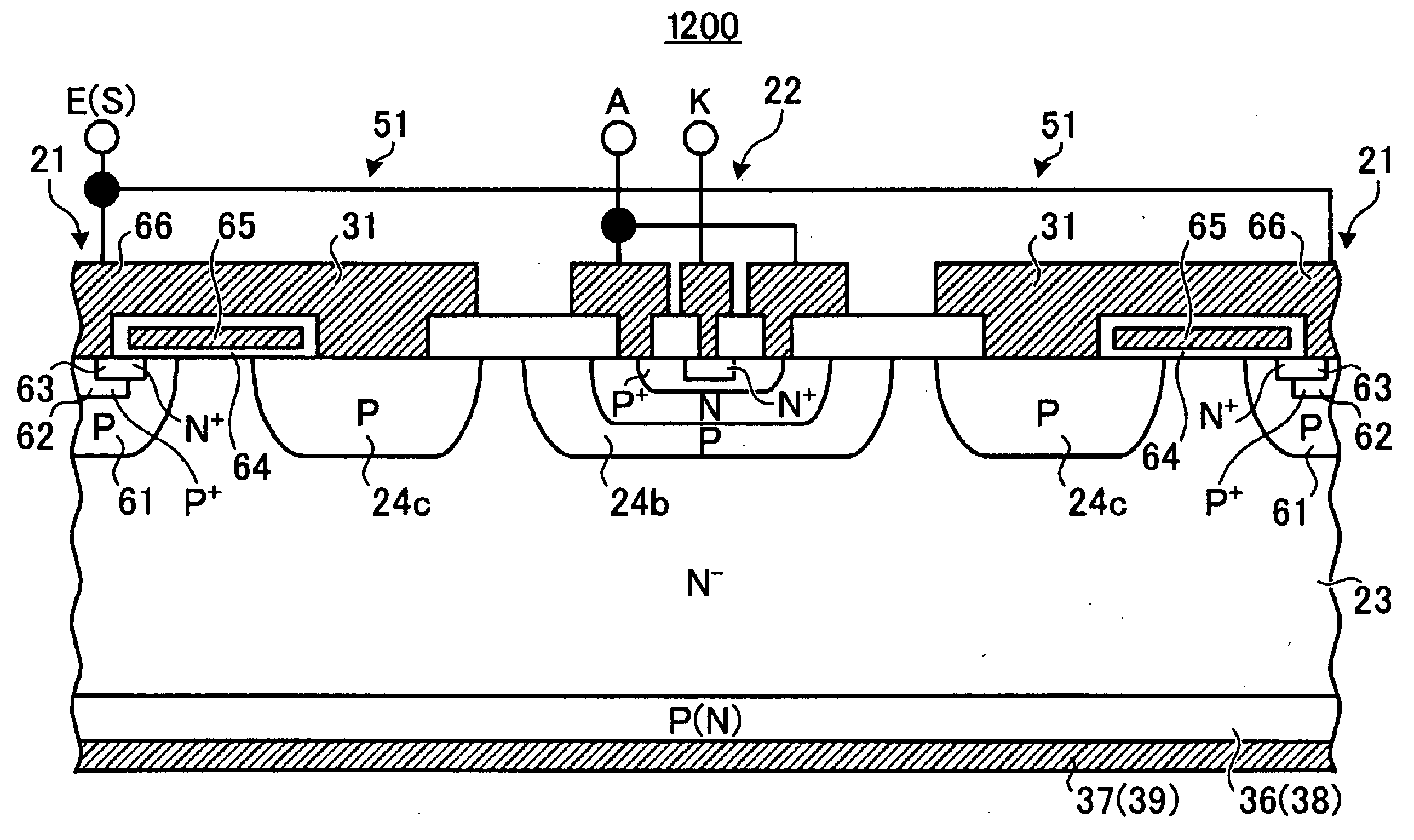
[0037]FIG. 3 is a sectional view showing the configuration of a semiconductor device according to Embodiment 1 of the invention. As shown in FIG. 3, the semiconductor device 100 has a first P well 24b provided as a second semiconductor region in a first principal surface of an N− drift layer 23 which is a first semiconductor layer. An N well 25 which is a third semiconductor region is provided in the first P well 24b. A temperature detecting diode (temperature detecting element) 22 is provided in the N well 25.
[0038]That is, a high-concentration P+ anode region 26 as a fourth semiconductor region and a high-concentration N+ cathode contact region 27 are provided in the N well 25. An anode electrode (A) is connected to the P+ anode region 26. A cathode electrode (K) is connected to the N+ cathode contact region 27. The N+ cathode contact region 27 is provided to bring the cathode electrode into low resistance contact with the N well 25 which serves as a cathode region. The semiconduc...
embodiment 2
[0044]FIG. 4 is a sectional view showing the configuration of a semiconductor device according to Embodiment 2 of the invention. As shown in FIG. 4, the semiconductor device 200 is configured in the same manner as the semiconductor device 100 according to Embodiment 1 shown in FIG. 3 except that a side of the N well 25 is surrounded by a trench gate structure 31 in place of the P+ high concentration region 28. Occurrence of latch-up in the transverse direction can be prevented because activation of a transverse NPN transistor can be completely prevented by this trench gate structure 31.
[0045]The trench gate structure 31 is provided in a terminal portion of the N well 25 in the first P well 24b. The trench gate structure 31 extends to be deeper than the N well 25. An insulating film 32 such as an oxide film is provided in a portion being in contact with a semiconductor of the trench gate structure 31, i.e. in an inner circumferential surface of the trench. The inside of the insulatin...
embodiment 3
[0046]FIG. 5 is a sectional view showing the configuration of a semiconductor device according to Embodiment 3 of the invention. As shown in FIG. 5, the semiconductor device 300 is a device including the temperature detecting diode 22 configured as shown in FIG. 3 and its peripheral structure. A first P well 24b however further extends in the transverse direction compared with the first P well 24b in Embodiment 1, so that the first P well 24b forms a hole extraction region 42 of a diverter 41. A high-concentration P+ contact region 43 is provided in a front surface of a part of the first P well 24b which forms the diverter 41. The hole extraction region 42 is set to have the same electric potential as the emitter (source) potential of the primary semiconductor element 21. With this configuration, the first P well 24b has the same electric potential as the emitter (source) potential. As a result, occurrence of latchup due to high dV / dt can be suppressed because voltage change (dV / dt)...
PUM
 Abstract
Description
Claims
Application Information