Method of Manufacturing III-Nitride Crystal, and Semiconductor Device Utilizing the Crystal

a manufacturing method and technology of iiinitride, which are applied in the direction of crystal growth process, polycrystalline material growth, transportation and packaging, etc., can solve the problems of superior crystallinity and inability to obtain superior crystallinity of gan crystal, and achieve superior crystallinity and light-emission efficiency. , the effect of superior crystallinity

Active Publication Date: 2009-09-24
SUMITOMO ELECTRIC IND LTD
View PDF22 Cites 70 Cited by
  • Summary
  • Abstract
  • Description
  • Claims
  • Application Information

AI Technical Summary

Benefits of technology

[0009]An object of the present invention, to resolve the problems discussed above, is to make available a method of manufacturing III-nitride crystal of superior crystallinity, having a major surface of plane orientation other than {0001}, designated by choice, and to make available semiconductor devices, utilizing III-nitride crystal obtained by the manufacturing method, that excel in light-emission efficiency.
[0013]The present invention enables the provision of a method of manufacturing III-nitride crystal of superior crystallinity, having a major surface of plane orientation other than {0001}, designated by choice, and the provision of semiconductor devices, utilizing III-nitride crystal obtained by the manufacturing method, that excel in light-emission efficiency.

Problems solved by technology

With the method in Pat. App. Pub. No. 2005-162526, however, inasmuch as growth of the GaN crystal is carried out with, as seeds, the masses of crystal GaN that have been embedded into the sapphire substrate, due to the disparity in thermal expansion coefficient between sapphire and GaN, fractures and strains appear in the GaN crystal when the crystal is cooled following the growth process, such that GaN crystal of superior crystallinity has not been obtainable.
Furthermore, if III-nitride crystal containing Al—for example, AlGayIn1-x-yN (x>0, y≧0, x+y≦1)—is grown by the method in Pat. App. Pub. No. 2005-162526, because the Al precursor is not selective with respect to the silicon oxide film, the AlxGayIn1-x-yN grows onto the silicon oxide film as well, and consequently AlxGayIn1-x-yN crystal of superior crystallinity has not been obtainable.

Method used


Image

  • Method of Manufacturing III-Nitride Crystal, and Semiconductor Device Utilizing the Crystal
  • Method of Manufacturing III-Nitride Crystal, and Semiconductor Device Utilizing the Crystal
  • Method of Manufacturing III-Nitride Crystal, and Semiconductor Device Utilizing the Crystal

Examples


embodiment 1

[0098]To begin with, referring to FIG. 3A, the (0001) face and (000-1) face—the two major surfaces—of GaN bulk crystal (III-nitride bulk crystal 1) were ground and polished to bring the roughness average Ra of either major surface to 5 nm. Here measurement of the surface roughness average Ra was carried out by AFM.

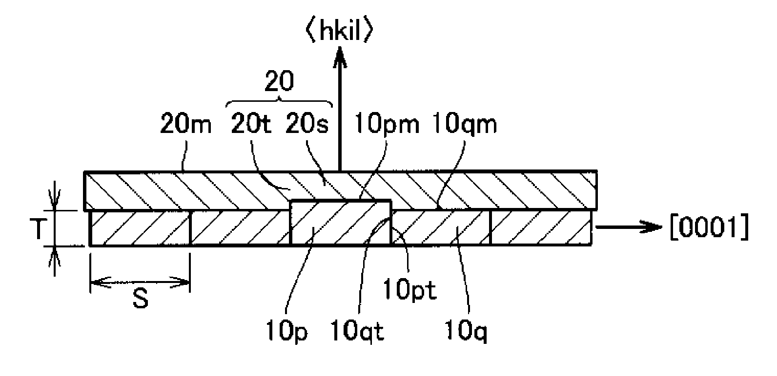
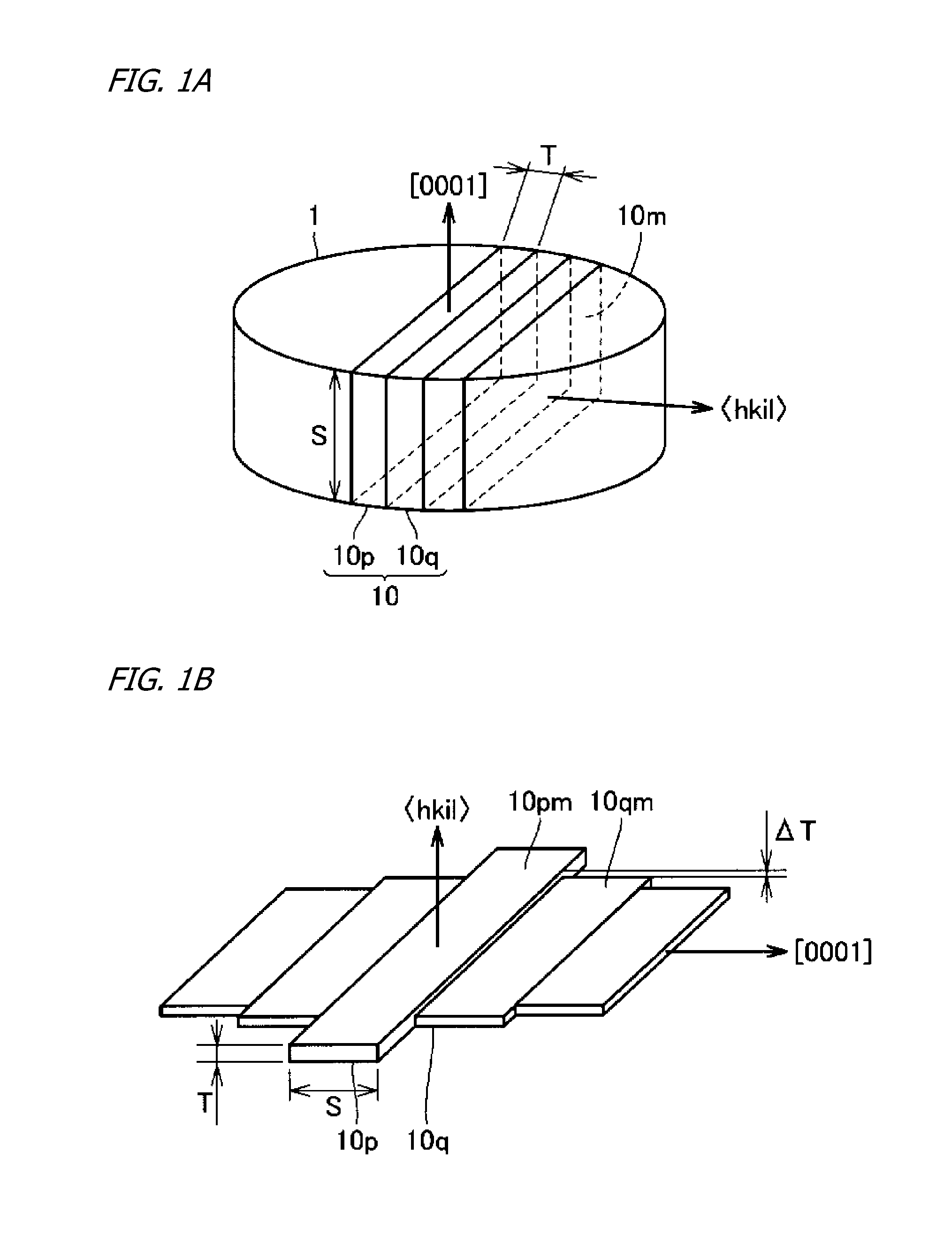
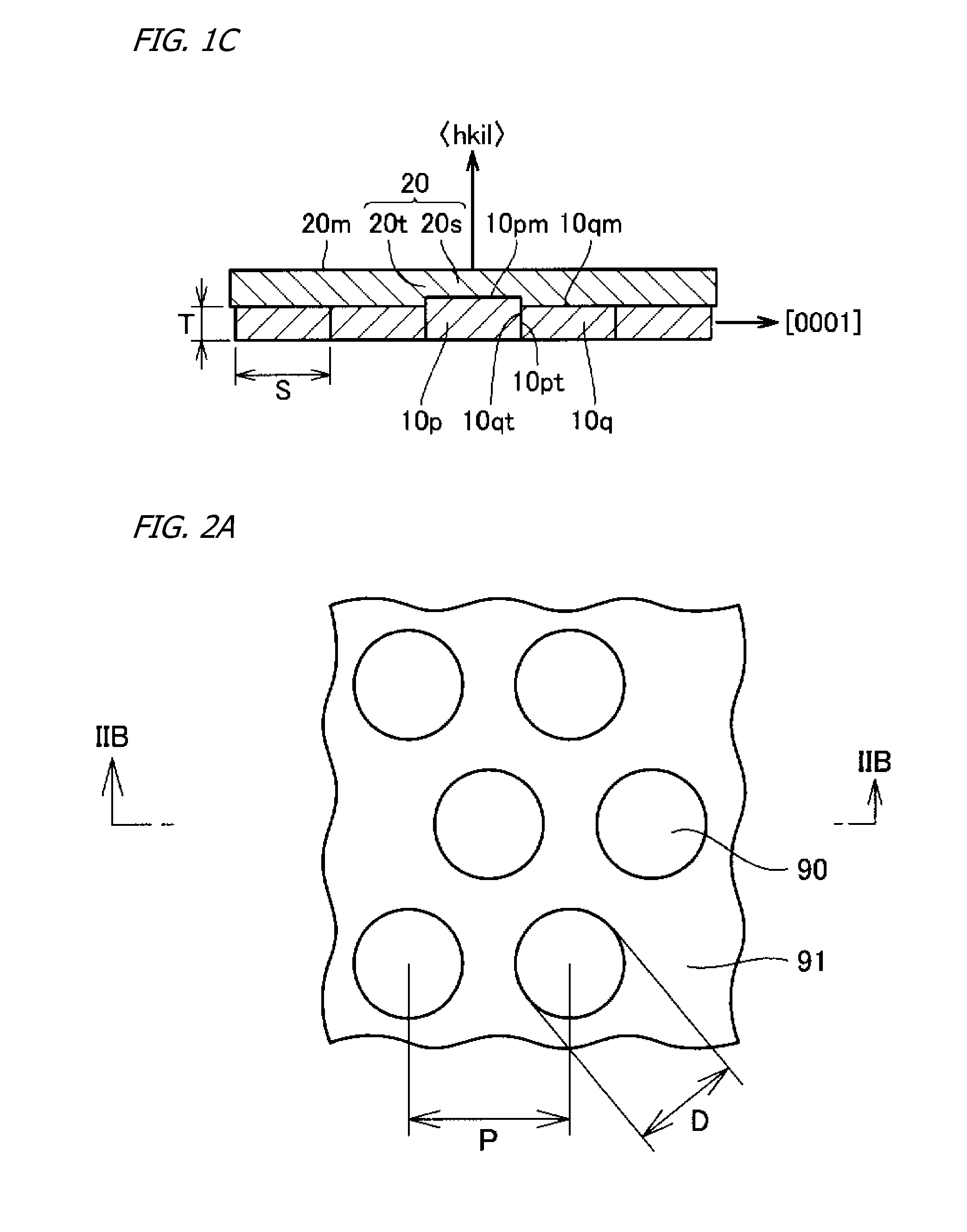
[0099]Next, referring to FIG. 3A, the GaN bulk crystal (III-nitride bulk crystal 1) whose roughness average Ra on either of its major surfaces had been made 5 nm was sawed along a plurality of planes perpendicular to a direction to slice off a plurality of GaN crystal substrates (III-nitride crystal substrates 10p, 10q) whose width S was 3 mm, length L was 20 to 50 mm, and thickness T was 1 mm, having {1-100} major surfaces. Subsequently, the not-ground and not-polished four sides of each sliced-off GaN crystal substrate were ground and polished, to bring the roughness average Ra of the four surfaces to 5 nm. A plurality of GaN crystal substrates whose roughness average R...

embodiment 2

[0105]Reference is again made to FIG. 3A: Apart from grinding and polishing the (0001) face and (000-1) face—the two major surfaces—of GaN bulk crystal (III-nitride bulk crystal 1) to bring the roughness average Ra of either major surface to 50 nm, in the same manner as in Embodiment 1, plural GaN crystal substrates (III-nitride crystal substrates 10p, 10q) were sliced off, and the not-ground and not-polished four sides of each GaN crystal substrate were ground and polished, to bring the roughness average Ra of the four surfaces to 5 nm. Among the plurality of GaN crystal substrates were GaN crystal substrates whose major-surface plane orientation did not coincide perfectly with {1-100}, but the plane orientation of the major surface of such GaN crystal substrates in all cases was misoriented by 5° or less with respect to {1-100}.

[0106]Next, referring to FIG. 3B, the plural GaN crystal substrates (III-nitride crystal substrates 10p, 10q) were situated in the same manner as in Embodi...

embodiment 3

[0111]To begin with, referring to FIG. 5A, the (0001) face and (000-1) face—the two major surfaces—of GaN bulk crystal (III-nitride bulk crystal 1) were ground and polished to bring the roughness average Ra of either major surface to 5 nm.

[0112]Next, again referring to FIG. 5A: The GaN bulk crystal (III-nitride bulk crystal 1) whose roughness average Ra on either of its major surfaces had been made 5 nm was sawed along a plurality of planes perpendicular to a direction to slice off a plurality of GaN crystal substrates (III-nitride crystal substrates 10p, 10q) whose width S was 3 mm, length L was 20 to 50 mm, and thickness T was 1 mm, having {11-20} major surfaces. Subsequently, the not-ground and not-polished four sides of each sliced-off GaN crystal substrate were ground and polished, to bring the roughness average Ra of the four surfaces to 5 nm. A plurality of GaN crystal substrates whose roughness average Ra on the {11-20} major surfaces was 5 nm was thus obtained. Among these...


PUM


Abstract

The present III-nitride crystal manufacturing method, a method of manufacturing a III-nitride crystal (20) having a major surface (20m) of plane orientation other than {0001}, designated by choice, includes: a step of slicing III-nitride bulk crystal (1) into a plurality of III-nitride crystal substrates (10p), (10q) having major surfaces (10pm), (10qm) of the designated plane orientation; a step of disposing the substrates (10p), (10q) adjoining each other sideways in such a way that the major surfaces (10pm), (10qm) of the substrates (10p), (10q) parallel each other and so that the [0001] directions in the substrates (10p), (10q) are oriented in the same way; and a step of growing III-nitride crystal (20) onto the major surfaces (10pm), (10qm) of the substrates (10p), (10q).

Description

BACKGROUND OF THE INVENTION[0001]1. Technical Field[0002]The present invention, involving Group-III nitride crystal manufacturing methods, relates to a method of manufacturing III-nitride crystal having a major surface of plane orientation other than {0001}, designated by choice, and to semiconductor devices utilizing the crystal.[0003]2. Description of the Related Art[0004]Group-III nitride crystals, which are employed advantageously in semiconductor electronic devices including light-emitting devices and semiconductor sensors, are ordinarily manufactured by growing crystal onto the major surface of a sapphire substrate having a (0001) plane major surface, or onto a GaAs substrate having a (111) A-plane major surface, by means of a vapor-phase technique such as hydride vapor-phase epitaxy (HVPE) or metalorganic chemical vapor deposition (MOCVD), or by flux growth or other liquid-phase technique. Consequently, ordinarily obtained III-nitride crystals have a major surface whose plane...

Claims


Application Information

Patent Timeline
Patent Type & Authority Applications(United States)
IPC IPC(8): H01L29/20H01L21/20
CPCY10T428/24752H01L21/02658H01L21/02389H01L29/2003C30B23/025C30B9/12C30B25/18H01L21/02433C30B25/20C30B29/406C30B29/403H01L29/045H01L21/0254C30B19/02C30B29/38H01L21/205
Inventor MIZUHARA, NAHOUEMATSU, KOJIMIYANAGA, MICHIMASATANIZAKI, KEISUKENAKAHATA, HIDEAKINAKAHATA, SEIJIOKAHISA, TAKUJI
Owner SUMITOMO ELECTRIC IND LTD
Why Eureka
Try Eureka